


+86 13603063656
In the evolution of printed circuit board technology, few geometric parameters appear deceptively simple yet exert such profound influence on reliability as the Minimum Annular Ring. As electronic devices race toward thinner profiles, higher interconnection density, and more aggressive cost targets, PCB designers and manufacturers are increasingly forced to operate at the very edge of physical and process capability.
High-density interconnect (HDI) structures, microvias, stacked vias, and ultra-fine pitch components leave almost no tolerance for error. In this environment, the Minimum Annular Ring quietly becomes one of the last structural safeguards between a robust interconnect and latent field failure. Shrink it too aggressively, and the risks multiply—drill breakout, copper separation, plating voids, and catastrophic open circuits. Overspecify it, and routing density, cost efficiency, and product competitiveness suffer.

Minimum Annular Ring
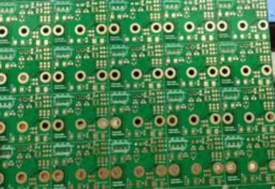
The Minimum Annular Ring refers to the smallest allowable width of copper that remains around a drilled hole or via after all manufacturing processes are completed. It is measured as the radial distance between the edge of the finished hole and the outer edge of the copper pad.
While the concept is simple in theory, its practical interpretation is more complex. The key word is minimum—not nominal, not average, but the worst-case scenario after drilling wander, layer misregistration, etching variation, and plating thickness distribution are all taken into account.
From a functional standpoint, the Minimum Annular Ring serves three essential purposes:
Electrical continuity between plated holes and copper features
Mechanical anchoring of the via barrel to the pad
Manufacturing tolerance buffer against unavoidable process variation
Without sufficient annular copper, even a perfectly plated via can become unreliable under thermal cycling or mechanical stress.
A frequent misunderstanding—especially among less experienced designers—is equating nominal pad dimensions with Minimum Annular Ring. In reality, the Minimum Annular Ring exists after everything goes wrong but still within process control.
Key contributors that reduce the effective annular ring include:
Drill bit positional tolerance
Drill entry and exit wander
Layer-to-layer misalignment
Etching undercut
Copper thickness variation
This is why seasoned PCB manufacturers insist that Minimum Annular Ring be treated as a statistical survival margin, not a design convenience.
As via diameters shrink and pad sizes are minimized to free routing space, the relative importance of the Minimum Annular Ring increases dramatically. In traditional through-hole designs, generous copper pads masked many process imperfections. In HDI and fine-line PCBs, there is no such luxury.
In my observation, many field failures traced back to via opens or intermittent connections share one root cause: annular ring erosion beyond the safe limit during fabrication.
The Minimum Annular Ring should never be selected in isolation. It is a central DFM parameter that interacts with:
Drill diameter selection
Pad stack definition
Layer count and registration strategy
Via type (through, blind, buried, microvia)
A robust design begins by recognizing that manufacturing capability sets the floor, not marketing ambition.
Design philosophies around the Minimum Annular Ring typically fall into two camps:
Conservative Design: Larger annular rings, higher yield, lower density
Aggressive Design: Smaller annular rings, higher density, tighter process control
Neither approach is inherently superior. The correct choice depends on product lifecycle, volume, reliability requirements, and supplier capability.
For mission-critical or long-life applications, I consistently recommend erring toward conservatism unless the manufacturing partner—such as JM PCB—can demonstrate proven control over drill registration and plating uniformity.
Different via structures impose different stresses on the annular ring:
Through-hole vias demand robust annular rings to absorb CTE mismatch
Blind vias rely heavily on pad adhesion to inner layers
Microvias depend on copper-to-copper bonding rather than mechanical anchoring
Attempting to apply a single Minimum Annular Ring value across all via types is a design shortcut that often leads to uneven reliability.
Reducing the annular ring increases available routing channels, but at a cost. The real challenge lies in identifying the point where routing density gains begin to compromise yield stability.
From experience, the most successful HDI designs are not those with the smallest annular rings—but those with intelligently varied annular ring sizes, adjusted according to via function and stress exposure.
Although the Minimum Annular Ring is often discussed from a mechanical or manufacturing standpoint, its influence on electrical performance is equally critical. At its core, the annular ring defines the electrical interface between planar copper features and the vertical plated via barrel. Any compromise in this interface introduces increased resistance, instability under load, or intermittent connectivity.
A sufficiently sized Minimum Annular Ring ensures:
Low and stable contact resistance
Uniform current transfer between layers
Reduced susceptibility to micro-cracking at the pad–barrel junction
When the annular ring is reduced below a stable threshold, the electrical margin narrows, especially in designs carrying higher current densities or fast-switching signals.
One often overlooked aspect is how the Minimum Annular Ring influences current density concentration. As the annular ring becomes smaller, current is forced through a reduced copper cross-section around the hole edge. This localized crowding can lead to:
Elevated Joule heating
Accelerated copper grain fatigue
Increased risk of electro-migration
In power-sensitive designs, such as DC-DC conversion boards or motor control PCBs, undersized annular rings can quietly become long-term reliability liabilities—even if the vias initially pass electrical testing.
For high-speed digital and RF designs, the Minimum Annular Ring indirectly affects signal integrity through geometry consistency. Variations in annular ring width alter the effective capacitance and inductance at via transitions.
While the impact of a single via may be small, in dense BGA fan-outs or high-layer-count backplanes, cumulative variation can result in:
Impedance discontinuities
Increased insertion loss
Reflection-induced eye closure
From my experience, signal integrity simulations often assume ideal via geometries. Designs that push the Minimum Annular Ring to extreme limits frequently deviate from these assumptions during fabrication, introducing performance gaps between simulation and reality.
Electroplated copper thickness is never perfectly uniform, particularly at the pad-to-barrel interface. A robust Minimum Annular Ring provides redundancy against localized thinning or voids.
When annular rings are too narrow, even minor plating non-uniformity can result in:
Reduced effective conductive area
Hot spots under transient loads
Early-life via failures during burn-in
Thus, from an electrical reliability standpoint, the Minimum Annular Ring functions as a current-sharing buffer, not merely a dimensional feature.
| Process Step | Typical Risk to Annular Ring | Mitigation Strategy |
|---|---|---|
| CNC drilling | Radial drill wander | Conservative pad sizing |
| Lamination | Layer misregistration | Registration compensation |
| Etching | Copper undercut | Controlled etch profiles |
| Plating | Thickness non-uniformity | Minimum copper redundancy |
| Depanelization | Localized stress | Reinforced pads in stress zones |
The Minimum Annular Ring is often treated as a constraint to be minimized, but in reality, it is a structural and electrical insurance policy embedded in every via. It absorbs manufacturing variation, distributes mechanical stress, stabilizes electrical performance, and protects long-term reliability.
In high-density PCB design and manufacturing, progress is often framed as a battle against physical limits—smaller vias, tighter spacing, thinner materials. Yet throughout this evolution, one truth remains unchanged: reliability is not achieved by ignoring limits, but by understanding them deeply.
The Minimum Annular Ring represents one of those limits that cannot be negotiated away. It is not a legacy constraint from older PCB technologies, nor a conservative artifact imposed by manufacturers. Instead, it is a practical expression of how geometry, materials, and processes interact under real-world conditions.
From a design perspective, the Minimum Annular Ring serves as a bridge between intent and execution. It translates theoretical layouts into manufacturable structures that can withstand drilling variation, layer misregistration, copper plating non-uniformity, and thermal stress over time. Designs that respect this bridge tend to scale smoothly from prototype to mass production. Designs that do not often pay the price later—through yield loss, field failures, or costly redesigns.
From a manufacturing standpoint, the Minimum Annular Ring is a stabilizer. It absorbs the natural variability inherent in even the most advanced fabrication processes. When designers and manufacturers align early on realistic annular ring targets, the result is not compromised innovation, but predictable, repeatable quality.
Mastering the Minimum Annular Ring is less about pushing it smaller and more about placing it intelligently. It is a strategic choice—one that reflects design maturity, supplier understanding, and long-term reliability thinking. In an industry where margins are thin and expectations are high, that maturity often makes the difference between a successful product and a fragile one.
Yes. Through-hole vias rely more on mechanical anchoring, while microvias depend on copper bonding. Each structure requires a tailored annular ring strategy.
HDI designs use smaller vias and pads, leaving less tolerance for drilling and registration errors. A reduced safety margin makes annular ring integrity essential for yield and reliability.
Yes. Marginal annular rings may maintain continuity during testing but fail later under thermal cycling, vibration, or mechanical stress.
A sufficient annular ring distributes stress between the via barrel and pad, reducing the risk of copper cracking or pad separation caused by CTE mismatch.
Not always. While it may increase routing space, excessive reduction often leads to yield loss and long-term reliability issues that outweigh density gains.


Connect to a Jerico Multilayer PCB engineer to support your project!
Request A Quote


 Quote
Quote