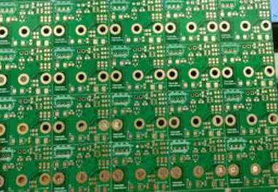
In modern printed circuit board design, performance margins are increasingly shaped not by headline technologies but by subtle geometric decisions made deep within the stack-up. One such decision—often underestimated yet profoundly influential—is the definition and control of antipad clearance. As signal speeds rise, layer counts increase, and thermal constraints tighten, antipad clearance becomes a balancing act between electrical integrity, manufacturability, and thermal behavior.

Antipad clearance
Antipad clearance refers to the intentional copper-free region surrounding a drilled hole or via within a conductive plane layer, such as a power or ground plane. Unlike pads, which establish electrical connection, antipads serve to isolate vias from planes unless an explicit connection is required.
Physically, the antipad creates a void in the copper plane. This void alters the local electromagnetic field distribution, capacitance, and current return paths. While the concept appears simple, its implications are multi-dimensional:
Electrical isolation and parasitic capacitance control
Thermal conduction interruption or moderation
Mechanical stress relief during lamination and thermal cycling
In practice, antipad clearance is not a single value but a design decision influenced by drill tolerance, layer registration, plating thickness, and the functional role of the via.
In multilayer PCBs, antipad clearance takes on greater complexity. Each plane layer may require a different antipad strategy depending on its electrical role and proximity to signal layers.
For example, a through-hole via passing through ten layers may require antipads on all non-connected planes, while a blind via may only require selective clearance. The cumulative effect of these clearances significantly influences plane integrity and impedance continuity.
From my experience, designers often reuse default antipad rules across all layers. This approach simplifies CAD workflows but ignores the nuanced behavior of electromagnetic coupling across the stack-up. In high-speed designs, such oversimplification often manifests as unexpected impedance dips or resonant noise issues late in validation.
One of the most critical electrical impacts of antipad clearance is its role in managing parasitic capacitance between vias and planes. Smaller clearances increase capacitance, which can slow edge rates and distort high-frequency signals.
At lower frequencies, this effect may be negligible. However, in multi-gigabit designs, even a few femtofarads of unintended capacitance can introduce measurable signal degradation. Enlarging antipad clearance reduces this capacitance but introduces trade-offs in plane continuity and thermal performance.
In my view, antipad clearance should be treated as a tuning knob rather than a fixed constraint. Simulation-driven optimization—rather than rule-based defaults—consistently yields better outcomes in dense, high-speed layouts.
Signal integrity is fundamentally about preserving waveform fidelity from source to receiver. Antipad clearance plays an indirect yet powerful role by shaping the electromagnetic environment around vias.
Improper antipad sizing can lead to:
Impedance discontinuities at layer transitions
Increased return path inductance
Mode conversion in differential signals
One subtle issue I have observed is over-aggressive antipad enlargement in the name of capacitance reduction. While electrically attractive, excessive clearance can disrupt return current paths on reference planes, paradoxically increasing noise and jitter.
| Design Dimension | Role of Antipad Clearance | Potential Risk if Mismanaged |
|---|---|---|
| Signal Integrity | Controls via-to-plane capacitance and impedance continuity | Reflections, jitter, eye closure |
| Power Integrity | Preserves plane isolation while maintaining copper continuity | Voltage drop, localized heating |
| Thermal Management | Limits or enables vertical heat transfer | Overheating or thermal bottlenecks |
| Mechanical Reliability | Reduces stress concentration around vias | Barrel cracking, pad cratering |
| EMI / EMC | Shapes return current paths and loop areas | Increased radiation and noise |
| Manufacturability | Provides tolerance for drilling and registration | Yield loss, shorts, opens |
Antipad clearance sits at the intersection of signal integrity, thermal management, and manufacturability. Optimizing it requires not only theoretical understanding but practical insight into fabrication realities. By balancing electrical isolation with plane continuity and thermal needs, designers can unlock higher performance margins without escalating cost or risk.
In high-speed, high-density, and high-reliability designs, antipad clearance operates at the intersection of multiple engineering disciplines. Electrically, it shapes parasitic capacitance, impedance continuity, and return current behavior. Thermally, it governs how heat flows—or is intentionally blocked—between layers. Mechanically, it affects stress distribution around vias during lamination and thermal cycling. Manufacturability-wise, it directly influences yield stability, registration tolerance, and long-term reliability.
What makes antipad clearance particularly challenging is that its effects are rarely isolated. Increasing clearance to reduce via capacitance may unintentionally weaken reference planes. Tightening clearance to preserve plane integrity may raise EMI risk or compromise drill tolerance. There is no universally “correct” value—only contextually optimized decisions.
From my own engineering perspective, the most mature PCB designs are those where antipad clearance is treated as a strategic lever rather than a static rule. These designs share several characteristics:
Antipad clearance is differentiated by via function, signal class, and layer role
Electrical and thermal objectives are evaluated together, not sequentially
Simulation is used to define safe operating windows, not absolute targets
Manufacturing partners are consulted early to align intent with capability
As PCB technology continues to evolve toward finer geometries and higher performance demands, antipad clearance will only grow in importance. Designers who understand its multidimensional role—and who resist the temptation to rely on inherited defaults—will be better positioned to deliver boards that are not only fast and compact, but also robust, manufacturable, and reliable.
In the end, optimizing antipad clearance is not about removing copper. It is about intelligently shaping absence—using voids to control fields, heat, and stress with the same precision traditionally reserved for copper itself.
2. How does antipad clearance affect via impedance?
Antipad clearance influences the parasitic capacitance between the via barrel and plane layers, directly impacting impedance continuity at layer transitions.
3. Can antipad clearance improve thermal isolation?
Yes. By removing copper around vias, antipads can reduce vertical heat conduction, which is useful in thermally sensitive regions.
4. Is larger antipad clearance always better for high-speed signals?
No. Excessive clearance can disrupt return current paths, increasing inductance and degrading signal integrity.
5. How does manufacturing tolerance affect antipad clearance design?
Drill wander, layer misregistration, and plating thickness all require designers to include safety margins in antipad sizing.
Connect to a Jerico Multilayer PCB engineer to support your project!
Request A Quote