


+86 13603063656
Thermal vias are plated through-holes designed to transfer heat from one layer of a PCB to another. They are typically placed beneath or around heat-generating components to improve thermal management.
Common applications include:
The main purpose of thermal vias is simple: move heat away from hot components as quickly and efficiently as possible. Without effective heat dissipation, excessive temperatures can shorten component life and reduce long-term reliability.
thermal vias
Many PCB failures are caused or accelerated by high temperatures:
In electronics, temperature is often the hidden enemy. A component operating continuously at 105°C may have only half the expected service life compared to a component running at 85°C.
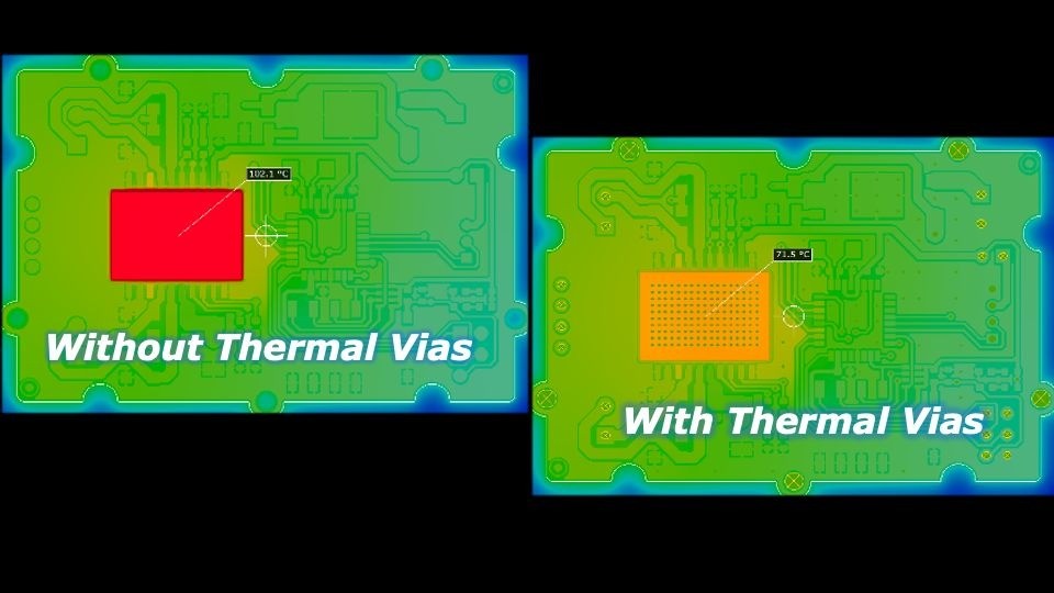
Thermal-vias provide a low-resistance path for heat to travel from hot components to inner or opposite layers of the PCB or to a heatsink. Properly designed thermal vias can:
Thermal management is a critical factor in PCB reliability. Implementing thermal vias correctly helps ensure your PCB performs consistently under demanding conditions, whether in automotive, industrial, or consumer electronics.
For PCB designers and engineers, understanding and applying thermal via strategies can mean the difference between a high-performing, reliable board and one that fails prematurely.
Thermal vias are used to transfer heat from high-power or heat-generating components to other PCB layers or heat sinks. They help lower component temperatures and improve long-term reliability.
The number of thermal vias depends on the power dissipation and available board space.
For most power devices, engineers typically use multiple vias arranged in an array beneath the thermal pad. More vias generally improve heat transfer, but excessive vias may increase manufacturing cost.
A common thermal via drill size ranges from 0.20 mm to 0.40 mm.
Smaller vias allow higher via density, while larger vias may improve heat transfer but consume more board space. The optimal size depends on the PCB design and manufacturing capability.
For BGA packages and exposed thermal pads, filled or plugged vias are often recommended to prevent solder wicking during assembly.
For general thermal management applications, open vias may be sufficient and can reduce manufacturing costs.
No.
Thermal vias improve heat transfer inside the PCB, but they do not replace external cooling solutions when dealing with high-power applications.
For significant heat loads, thermal vias are usually combined with:


Connect to a Jerico Multilayer PCB engineer to support your project!
Request A Quote


 Quote
Quote