


+86 13603063656
In modern electronics manufacturing, printed circuit boards (PCBs) serve as the foundation of virtually every device we interact with. From smartphones and smart appliances to advanced automotive control units and aerospace instrumentation, PCBs underpin the world’s technological progress. As the complexity and density of PCBs have grown, so has the demand for more precise, automated inspection methods to ensure quality and consistency. One of the most powerful tools for achieving these objectives is Automated Optical Inspection (AOI Testing).
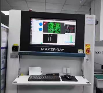
AOI Testing is a non-contact, camera-based inspection technique that uses high-resolution imaging and intelligent algorithms to examine PCBs for manufacturing defects. It compares each board to a predefined reference, identifying deviations such as open circuits, shorts, insufficient solder, incorrect component placement, and even subtle cosmetic defects. By performing these checks automatically, AOI Testing drastically reduces human error and inspection time while simultaneously boosting yield and lowering costs.
This article aims to offer an in-depth exploration of AOI Testing—its principles, advantages, process flow, and its transformative impact on PCB manufacturing economics. In addition, we will highlight how forward-thinking PCB manufacturers such as JM PCB integrate AOI Testing into their operations to achieve industry-leading quality. Finally, readers will find five frequently asked questions (FAQs) at the end of this article to clarify common doubts about PCBs and related processes, including copper foil differences and inspection standards.

AOI Testing
The origins of AOI Testing can be traced back to the early days of mass electronics manufacturing when quality control relied heavily on manual inspection and rudimentary testing tools. As PCB designs grew denser, manual inspection quickly became inefficient, error-prone, and costly. This environment created the perfect opportunity for automation technologies to step in.
The first AOI Testing systems emerged in the 1980s, initially designed to check for simple flaws such as missing components or misalignments. These early systems used relatively low-resolution cameras and limited processing power. While groundbreaking at the time, their scope was restricted compared to what modern AOI Testing systems can do today.
Modern AOI Testing represents a quantum leap forward. Equipped with ultra-high-resolution cameras, multi-angle lighting systems, and advanced image-processing algorithms, these systems can detect defects at the micron level. They can differentiate between acceptable manufacturing variances and true defects, drastically reducing false positives. With machine learning increasingly integrated into AOI Testing, the systems can even improve themselves over time, learning from past inspections to increase accuracy and efficiency.
The adoption of AOI Testing also mirrors the rise of lean manufacturing and Six Sigma principles in electronics production. These methodologies emphasize defect prevention and process optimization—goals that AOI Testing aligns with perfectly. As a result, AOI Testing has shifted from being a “nice-to-have” to a critical, standard component of modern PCB manufacturing.
From a broader perspective, AOI Testing embodies the convergence of optics, computing, and manufacturing science. It highlights how interdisciplinary innovation drives progress in electronics production. For PCB manufacturers, this evolution has translated into measurable gains in yield, lower production costs, and improved customer satisfaction.
One of the most compelling reasons for implementing AOI Testing in the PCB manufacturing process is its ability to boost yield—the proportion of boards produced without defects relative to the total produced. In high-volume PCB production, even a small percentage increase in yield translates into substantial cost savings and improved profitability.
AOI Testing boosts yield by catching defects early in the manufacturing process, before they can propagate downstream. This early detection is especially crucial in complex multilayer boards where rework can be both technically challenging and expensive. By identifying issues such as solder bridging, missing components, or trace breaks at an early stage, AOI Testing prevents defective boards from consuming additional assembly time, materials, and labor.
Another way AOI Testing enhances yield is by providing process feedback. Modern systems can collect detailed defect data and feed it back into the manufacturing line in real time. For example, if a pick-and-place machine is misplacing a specific component, AOI Testing will flag the issue, enabling operators to adjust the equipment before the problem escalates. This closed-loop feedback mechanism not only reduces scrap but also improves process stability over time.
Manufacturers who embrace AOI Testing often find themselves better positioned to meet tight delivery schedules and high customer expectations. They can confidently guarantee the quality of each board, reducing the risk of costly returns or warranty claims. For industries like aerospace, automotive, and medical devices—where failure is not an option—AOI Testing becomes indispensable.
The yield improvements achieved with AOI Testing also extend to new product introductions (NPIs). During the prototype and pilot-run stages, AOI Testing helps engineers identify design-for-manufacturing (DFM) issues quickly. By catching these issues before mass production, companies can launch new products faster and with fewer quality problems.
While yield improvement and cost reduction often go hand in hand, it is worth examining how AOI Testing directly contributes to cutting costs in PCB manufacturing. The traditional cost drivers in PCB production include material waste, labor hours, rework expenses, and warranty claims. AOI Testing impacts all these areas simultaneously.
First, AOI Testing reduces the cost of rework and scrap. By identifying defective boards at the earliest possible stage, it minimizes the number of defective PCBs advancing to costly assembly or packaging steps. This early intervention translates to significant material savings, especially when dealing with expensive components or specialty boards.
Second, AOI Testing lowers labor costs. Automated inspection systems can examine boards far faster than human inspectors, and they operate continuously without fatigue. This efficiency allows manufacturers to reallocate labor to higher-value tasks such as process improvement, engineering, or customer service. In high-volume environments, the cost savings can be dramatic.
Third, AOI Testing minimizes the costs associated with customer returns and field failures. Defective PCBs that escape inspection can lead to product malfunctions, damaging brand reputation and incurring costly warranty or recall expenses. By catching defects before shipment, AOI Testing acts as an insurance policy against these financial risks.
Finally, AOI Testing improves operational efficiency. By providing rich data analytics on defect types, locations, and trends, it empowers managers to make informed decisions about equipment maintenance, supplier quality, and process optimization. These insights can lead to long-term cost reductions far exceeding the initial investment in AOI Testing equipment.
It is not uncommon for manufacturers to achieve a full return on investment (ROI) for AOI Testing systems within a year of deployment. This rapid ROI underscores the strategic value of AOI Testing in modern PCB manufacturing.
Understanding the process flow of AOI Testing helps demystify how it fits into a PCB production line. Although the specifics vary depending on the manufacturer and the type of PCB being produced, the following steps outline a typical AOI Testing process:
Image Acquisition: High-resolution cameras scan the PCB from multiple angles. Advanced systems use structured lighting and 3D imaging to capture detailed surface information, including component height and solder fillet profiles.
Reference Comparison: The captured images are compared against a “golden board” or digital reference model. This model represents the ideal PCB without defects.
Defect Detection Algorithms: Sophisticated software analyzes differences between the inspected board and the reference. Algorithms classify potential defects, separating critical errors (like shorts) from minor variances.
Defect Verification: In some cases, flagged anomalies undergo secondary verification either automatically or via a human operator to minimize false positives.
Reporting and Feedback: AOI Testing systems generate detailed inspection reports and feed defect data back to upstream processes, enabling corrective action.
Decision and Sorting: Boards are automatically sorted into “pass” and “fail” bins, with failed boards routed for rework or scrap depending on severity.
Modern AOI Testing systems integrate seamlessly with manufacturing execution systems (MES) and other factory software, allowing real-time traceability of inspection results. This digital connectivity is vital for companies pursuing Industry 4.0 initiatives and smart-factory goals.
One notable case study involves JM PCB, which has invested heavily in advanced AOI Testing systems. By embedding AOI Testing at multiple stages of their production line—such as post-solder paste application, post-assembly, and final inspection—JM PCB has significantly reduced defect rates and improved delivery reliability. Their approach demonstrates how AOI Testing can be a cornerstone of competitive differentiation in the PCB market.
The advantages of AOI Testing are multi-layered. Beyond the immediate benefits of defect detection, AOI Testing strengthens the entire production ecosystem, from supply chain quality to end-user satisfaction.
Early Defect Detection
AOI Testing’s greatest advantage lies in its ability to identify defects early. When PCBs leave the manufacturing line without inspection, small defects can snowball into significant downstream failures. AOI Testing provides a powerful safeguard against these latent issues by pinpointing anomalies before they propagate.
Higher Consistency and Accuracy
Manual inspection is inherently subjective and varies with inspector experience and fatigue levels. AOI Testing uses standardized algorithms, delivering consistent, repeatable results 24/7. This consistency builds confidence in both internal quality teams and external customers.
Real-Time Feedback Loop
AOI Testing systems can interface with pick-and-place, solder paste, or drilling equipment. This closed-loop system means a defect discovered by AOI Testing can trigger automatic adjustments upstream, reducing the chance of similar defects in subsequent boards.
Traceability and Compliance
Many industries—especially automotive, aerospace, and medical electronics—require traceable inspection data. AOI Testing generates detailed reports that become part of a product’s quality record, simplifying compliance with standards like ISO 9001 or IPC Class 3.
Reduced Human Error
By offloading inspection duties to a reliable automated system, manufacturers dramatically lower the probability of missed defects due to operator oversight. The system also frees skilled technicians to focus on more value-added tasks, such as process optimization or customer service.
Enhanced Customer Satisfaction
When AOI Testing ensures consistent quality, customers notice. Reduced field failures, fewer returns, and stable product performance enhance the manufacturer’s reputation. In a competitive industry, the ability to guarantee quality becomes a powerful differentiator.
Supports Continuous Improvement Initiatives
The defect data generated by AOI-Testing is invaluable for root-cause analysis. Over time, manufacturers can refine processes, improve supplier quality, and implement design changes informed by real-world inspection results.
While AOI Testing is powerful, it is most effective when integrated with other inspection and test methods. No single technique can catch every defect type; therefore, a layered inspection strategy is best practice.
Solder Paste Inspection (SPI): Performed before components are placed, SPI checks the volume and placement of solder paste deposits. Coupled with AOI Testing after placement, this approach prevents solder-related defects.
In-Circuit Testing (ICT): ICT validates the electrical functionality of PCBs by probing test points. AOI Testing can catch physical defects before ICT, ensuring only boards with a high probability of passing electrical tests proceed.
X-Ray Inspection: For hidden joints, such as BGAs (ball grid arrays), AOI Testing alone cannot see beneath components. X-ray inspection complements AOI Testing by revealing hidden solder voids or bridging.
Functional Testing: Once assembly is complete, functional testing ensures the board performs as intended. AOI Testing’s role here is to eliminate obvious mechanical and optical defects before functional tests begin.
This integrated approach is sometimes referred to as a “test pyramid,” with AOI Testing serving as a key middle layer. By placing AOI Testing at multiple points—post-solder paste, post-placement, post-reflow, and final inspection—manufacturers achieve a holistic quality assurance system.
One overlooked benefit of AOI-Testing is its contribution to sustainability. By catching defects early and reducing scrap, AOI-Testing directly lowers material waste. This is particularly important as electronics manufacturing faces growing scrutiny over its environmental footprint.
AOI Testing also reduces the need for energy-intensive rework processes such as desoldering or remanufacturing. In high-volume production, these small savings add up to a significant reduction in energy use and waste generation. As environmental regulations tighten worldwide, AOI-Testing helps manufacturers stay compliant while aligning with corporate sustainability goals.
Even the most advanced AOI-Testing systems cannot succeed without proper human integration. Operators and engineers must understand how to set inspection parameters, interpret results, and take corrective actions.
Best practices include:
Comprehensive Training: Teaching staff how AOI-Testing works, what each defect category means, and how to adjust machines accordingly.
Cross-Functional Teams: Involving quality engineers, production managers, and line operators in AOI-Testing review meetings ensures everyone shares ownership of quality.
Continuous Feedback: Using AOI-Testing reports as a living document to drive weekly or daily process improvements.
By empowering employees to use AOI-Testing data proactively, manufacturers turn the inspection step into a knowledge hub rather than a bottleneck.
In the high-stakes world of electronics manufacturing, boosting yield and cutting costs are no longer optional — they are existential requirements. AOI-Testing stands out as one of the most effective ways to achieve both simultaneously. By combining precise optical inspection with real-time analytics and feedback loops, AOI-Testing transforms quality assurance from a back-end checkpoint into a front-line strategy.
Across this article, we’ve examined how AOI-Testing:
Detects defects early to improve yield
Cuts costs through reduced rework, labor savings, and fewer field failures
Integrates with other inspection techniques for comprehensive coverage
Supports smart manufacturing and sustainability goals
Strengthens supply chain quality and compliance
We’ve also seen how JM PCB leverages AOI-Testing to set itself apart in a competitive industry, using the technology not just for inspection but as a foundation for continuous improvement. Their example shows how AOI-Testing can evolve from a technical tool to a strategic differentiator.
My own reflection is that AOI-Testing represents more than a technology shift; it embodies a mindset change. It pushes manufacturers to think of quality as a dynamic, data-driven process rather than a static end-of-line check. In doing so, AOI-Testing elevates both the technical and cultural maturity of an organization.
For PCB manufacturers striving to remain competitive, AOI-Testing is no longer optional. It is an essential ingredient in the recipe for reliability, efficiency, and customer trust. By adopting AOI Testing thoughtfully and fully, companies position themselves not just to survive but to thrive in the increasingly demanding world of electronics manufacturing.Frequently Asked Questions
FAQ 1: What is AOI-Testing and why is it important in PCB manufacturing?
AOI-Testing (Automated Optical Inspection) uses high-resolution cameras and software algorithms to inspect PCBs for defects such as shorts, opens, misalignments, or insufficient solder. It is critical because it provides fast, repeatable, and objective inspection results, reducing scrap and rework costs while improving yield.
FAQ 2: What is the difference between rolled copper foil and electrolytic copper foil?
Rolled copper foil is produced by mechanically rolling copper into thin sheets, offering better surface quality, lower roughness, and higher mechanical strength—making it ideal for flexible PCBs. Electrolytic copper foil is deposited via an electrolytic process and is more flexible and cost-effective, commonly used for rigid PCBs.
FAQ 3: How does AOI-Testing compare with manual inspection?
Manual inspection depends on human vision and concentration, which can vary and degrade over time. AOI-Testing provides a standardized, automated approach that detects smaller defects more consistently, operating at speeds far beyond human capability.
FAQ 4: At which stage of PCB manufacturing should AOI-Testing be implemented?
AOI-Testing can be implemented at multiple stages: after solder paste printing, after component placement, after solder reflow, and during final inspection. Using AOI Testing at several checkpoints maximizes defect detection and process feedback.
FAQ 5: How does AOI-Testing support high-reliability industries like aerospace or medical electronics?
These industries require strict quality standards (often IPC Class 3 or higher). AOI-Testing provides detailed, traceable inspection data to meet these requirements and reduce the risk of field failures. Its ability to detect subtle defects early makes it essential for mission-critical applications.


Connect to a Jerico Multilayer PCB engineer to support your project!
Request A Quote


 Quote
Quote