


+86 13603063656
In the era of high-speed, high-density, and increasingly multilayer electronic systems, the role of micro-manufacturing technologies has grown from supportive to absolutely foundational. Among the many advanced processes that govern signal integrity and structural precision in printed circuit boards, the technique known as Backdrill has emerged as one of the most important.
Backdrill is not a flashy topic, yet it sits at the core of every high-speed networking device, every 5G baseband board, every aerospace controller, and every server-grade computing module. As signaling frequencies rise and interconnect density becomes more extreme, unused copper barrel segments—called stubs—pose growing risks to timing accuracy, reflections, crosstalk, radiation, and loss. Backdrill offers an elegant and highly practical solution by selectively removing these unwanted via structures, enabling deeper electrical precision while maintaining manufacturability.

Backdrill
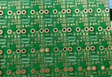
Backdrill is a subtractive drilling process used in PCB manufacturing to remove the unused portion of a plated through-hole (PTH) via barrel. These unused segments—called via stubs—exist below the last connected inner-layer pad. Because high-speed signals do not utilize the lower part of the via, that structure becomes a liability rather than an asset.
Backdrilling selectively mills away the lower part of the via barrel to eliminate these stubs, leaving the via electrically shorter and significantly more stable at higher frequencies.
A standard plated-through via connects multiple PCB layers, but not every layer uses the entire via length. The unused length acts like a small unterminated transmission line that reflects high-frequency signals. Backdrill removes this unused section so the via behaves more like an ideal interconnect.
High-speed signals hate discontinuities.
A via stub is essentially a resonating copper antenna.
The higher the frequency, the worse the distortion.
It uses a mechanical drill with a diameter slightly larger than the original via drill.
It must stop within a very controlled depth to avoid damaging functional pads.
It must be programmed precisely using stack-up information and layer registration.
From an electromagnetic perspective, a via stub behaves like an open-ended resonator. When a high-frequency signal enters the via, part of the wave energy leaks into the stub, travels to the open end, and reflects back.
This means even a small stub can cause distortion at common operating frequencies of gigabit-level devices.
For example:
A 0.5 mm stub resonates near ~15 GHz
A 1.0 mm stub resonates near ~7.5 GHz
A 2.0 mm stub resonates near ~3.8 GHz
This places Backdrill as an essential technique for:
10G Ethernet
25G / 50G transceivers
56G PAM4
112G SerDes
PCIe Gen4/Gen5/Gen6
DDR4/DDR5 memory channels
Whenever stub length exceeds ~10% of the signal rise time requirement, Backdrill becomes mandatory.
Backdrill was originally developed for military and aerospace PCBs, where signal integrity requirements demanded extreme levels of precision. As data centers and 5G networks entered the era of multi-gigabit transmission, Backdrill migrated into commercial production.
Early era – Manual drill depth calibration, ±6–8 mil variation
Transitional era – Laser depth measurement, improved drill bits, ±3–4 mil variation
Modern era –
CNC drilling with real-time Z-axis feedback
3D topography mapping of copper layers
Controlled depth algorithms
Backdrill hole quality inspection with X-ray AOI
±1–2 mil depth precision
Today, Backdrill is no longer a specialty process but a mainstream requirement for almost any high-speed multilayer PCB.
Backdrill reduces or eliminates via stubs, which directly improves signal transmission in several ways:
Reduced reflections
Lower insertion loss
More consistent impedance profiles
Better timing accuracy
Cleaner eye diagrams in high-speed communication
Modern PCB designers often underestimate the cumulative effect of multiple stubs along a critical channel. Even if one stub is short, six or seven stubs in sequence—from vias, connectors, and crossovers—can degrade margins enough to fail at high data rates. Backdrill helps maintain reliability without needing to redesign the entire routing architecture.
Via stubs behave like miniature antennas, radiating energy and coupling noise. Backdrilling reduces these antennas, shrinking their effective radiating area and reducing:
Far-end crosstalk
Near-end crosstalk
Radiation emissions
Spurious harmonics
This is especially beneficial in:
Dense backplane PCBs
Telecom base station boards
High-current automotive electronics
Backdrill removes excess copper in regions where thermal or mechanical stress could accumulate. Benefits include:
Lower risk of plating cracks at the stub end
Improved fatigue life during temperature cycling
Reduced risk of barrel-to-pad separation
Better solder joint stability for large connectors
In some mechanical environments—high-vibration, wide-temperature-range industries—Backdrill can increase PCB lifetime significantly.
Back-drill performance depends not only on drill accuracy but also on the physical, chemical, and mechanical characteristics of the PCB materials involved. The interaction between the drill bit and the substrate determines the drill speed, cut quality, resin residue, and, ultimately, the integrity of the hole after Back-drill.
This section analyzes how material choices influence Back-drill results and what designers should consider when targeting high-speed, multilayer stack-ups.
Different resin systems exhibit different hardness, brittleness, and heat response characteristics. These affect drilling outcomes significantly.
| Resin System | Hardness | Backdrill Impact |
|---|---|---|
| Standard FR-4 | Medium | Predictable drilling, moderate smear |
| High-Tg FR-4 | Higher | Cleaner cuts, less deformation |
| Low-loss resins (e.g., Panasonic Megtron) | Varies | Softer, prone to smear if speed is high |
| PTFE materials | Very soft | Requires low torque, risk of fiber pull-out |
| Polyimide | Hard | Generates heat, needs slower drilling |
Soft resins require slower drill speed and more precise feed control, while hard resins require reduced torque to avoid thermal buildup. Many Backdrill failures in industry—especially pad breakout or glass weave exposure—are connected more to material characteristics than to drill parameter misconfigurations. IPC-compliant materials help, but stacking different materials complicates Backdrill behavior dramatically.
Copper thickness determines:
Drill wear rate
Barrel integrity
Cone shape quality
Stub removal completeness
Drill bit may skid
Burr formation increases
Backdrill risk to inner pads rises
Barrel wall may collapse
Cone shape may be uneven
Designers must coordinate with manufacturers early to define plating thickness that balances electrical performance and Back-drill manufacturability.
Back-drill plays a foundational role in modern multilayer PCB fabrication. Its primary purpose—removing unnecessary copper stubs—has direct benefits for high-speed signal integrity, reliability, and low-loss performance. As digital systems move into 100+ Gbps territory, Backdrill is not just a “recommended” technique but, in many designs, a mandatory requirement.
In an era of increasing electrical complexity and shrinking SI margins, Backdrill represents a rare combination of low cost, high precision, and broad applicability across server, telecom, aerospace, and automotive sectors. Factories with disciplined process control, such as JM PCB, deliver consistent results that significantly reduce the risk of manufacturing defects.
Back-drill continues to evolve through AI-driven process control and advanced CNC systems. Designers who understand Backdrill deeply—and who apply it strategically—gain a powerful advantage in building reliable, high-speed, next-generation electronics.
It adds cost due to extra drilling time and inspection, but often reduces total system cost by preventing SI issues, reducing redesign cycles, and improving reliability.
By removing unused via segments, Backdrill reduces stub resonance, improves return loss, and minimizes signal reflection—critical for high-speed differential pairs.
Not always. It is essential for high-speed designs, telecom backplanes, and server boards but may be unnecessary for low-speed consumer electronics.
Yes, if overshoot is too large. Proper Z-axis calibration and drill parameter control are essential to protect active layers.
For high-speed applications, the goal is typically < 10 mil. For ultra-high-speed interfaces, < 5 mil is preferred.


Connect to a Jerico Multilayer PCB engineer to support your project!
Request A Quote


 Quote
Quote