


+86 13603063656

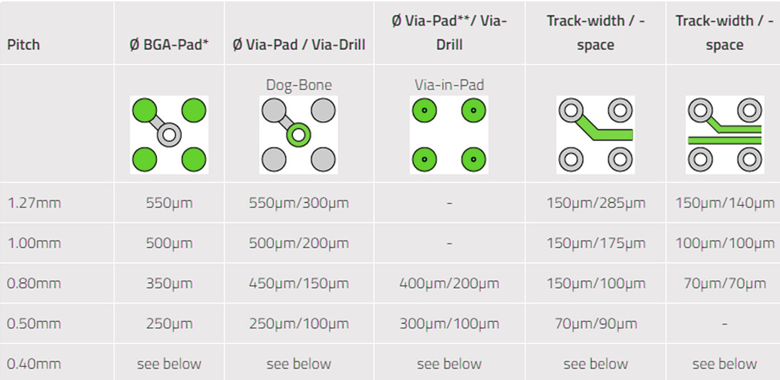
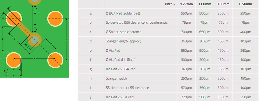
The values given are design proposals, values of component data sheets are always preferable.
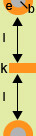
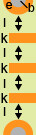
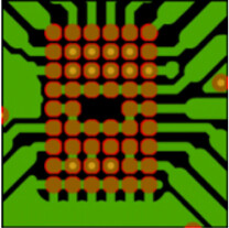
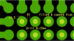
BGA with 0.4mm Pitch Via-in-Pad (Filled & Capped Vias)
Drill: 0.15mm
Annular ring: 84.5µm
Via-Pad: 319µm
Copper to copper: 81µm
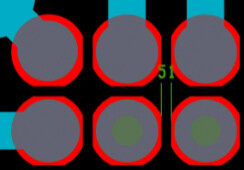
Solder-stop bridge: 51µm
Solder-stop clearance: 19µm
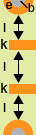
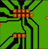
Routing of 0.4mm pitch BGA with maximum parameters.
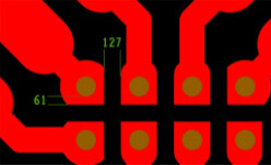
Drill: 0.15mm
Annular ring: varying, min. 61µm
Via-Pad: varying
Copper to copper: 127µm


Connect to a Jerico Multilayer PCB engineer to support your project!
Request A Quote


 Quote
Quote