


+86 13603063656
Multilayer PCBs go a long way in minimizing electromagnetic emissions, crosstalk, external wiring and weight of the circuit. However, while creating a PCB stack look straightforward, there is a lot more to it than what meets the eye.
Before we delve into how to build a multilayer PCB stack, let’s take a quick look at what they are and why they matter.
A multilayer printed circuit board (PCB) has more than two layers stacked with at least three conductive copper foil layers. However, they are not to be confused with double-sided PCBs, which only have two conductive layers of material.
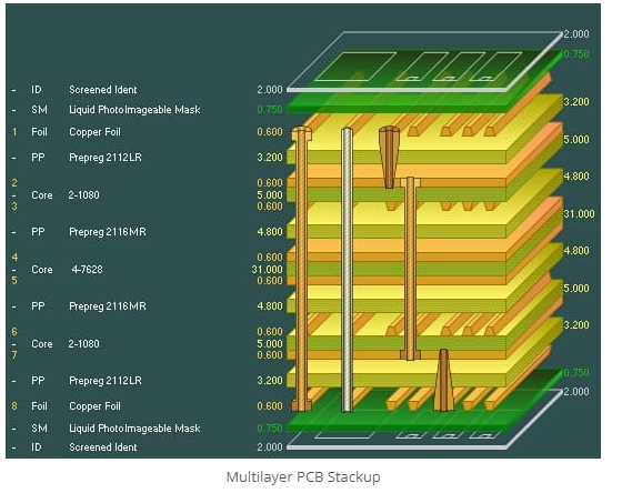
The most important part of designing a PCB is stack-up, which entails constructing the multiple layers of the PCB sequentially. It gives essential information on the copper weight, the material thickness required for the PCB manufacture, and the trace width for different controlled impedance traces developed.
A PCB stack-up consists of three main elements:
Metal Foil
A plane made up of conductive material, mainly copper, from which the circuits of the PCB are formed.
Prepreg
A dialectic material made from interwoven glass cloth infused with semi-cured-epoxy resin.
Copper-clad laminate
Also known as a core, a copper-clad laminate consists of one or several bonded prepreg plies with the top and bottom layers covered in copper foil.
High-density interconnect (HDI) stack-ups, on the other hand, are printed circuit boards that offer a greater wiring density/unit area. They typically have high signal performance considerations and come with micro vias, buried vias, blind vias, and built-up laminations.
When the copper layer is connected to the power supply, it becomes a power plane, providing the PCB with a steady voltage. In this case, it becomes a designated voltage common collector (VCC). Conversely, when connected to the common ground plane, the copper layer becomes the ground layer of the PCB stack up.
Using power and ground planes in PCBs offers several advantages, including:
PCB lamination is simply the process of subjecting the stack-up to extreme temperature and pressure conditions to permanently bond the metal foil and prepreg to the inner layers of the base PCB. Based on the chosen PCB materials, the exact temperature and pressure needed for the lamination process are selected from the datasheets.
Sequential lamination entails inserting dielectric material; usually, an epoxy pre-impregnated fiberglass sheet, between the laminated layers of the PCB and copper sheets.
The thickness of PCBs varies depending on their applications. It is determined by several factors, including the thickness of copper materials, operating environment, and the number of layers on the PCBs.
Conventional board thicknesses are around 62 mils (1.57mm). On the other hand, new standard thicknesses by manufacturers are 93mils (2.36mm) and 125 mils (3.17mm) which is 150% and 200% thicker than standard boards.
With electronic devices becoming more sophisticated, incorporating complex circuits onto a single-layer PCB is very difficult. However, it’s nothing adding multiple layers to a PCB stack-up can’t fix.
Multilayer PCBs have several advantages, and these include the following:
Start by selecting the inner core specifications obtained from the stack-up. These include the thickness and weight of copper, the type of epoxy glass used, and the panel size. Once done, the inner layers can be chemically or mechanically cleaned to remove contaminants on the copper surface.
An imaging material will be placed on the copper surface, covering the desired circuitry to expose unwanted copper. To show the desired copper circuitry, chemical etching is removed to remove unwanted copper before photoresist is stripped off.
The circuit is inspected to detect flows that are not visible to the human eye, such as opens and shorts in inner layers.
To enhance adhesion and the overall strength and board reliability board, exposed copper circuitry on the inner layer of the PCB is treated. The coating will now be complete.
For the subsequent layers, all steps listed above will be repeated.
The layers are stacked up, pressed, and heated in a vacuum chamber. The vacuuming removes all gases and trapped air within the layers before heat and pressure is applied to induce molecular bonding, laminating the multilayer PCB.
To create vias and through holes, the board is drilled. However, burrs – the copper parts left protruding during drilling, may be formed. These are removed during deburring, which also eliminates fingerprints on the copper surface.
Desmearing is then carried out to remove friction-melted resin formed during drilling by immersing the PCB into a series of chemicals or plasma treating.
Once desmeared, the drill holes are copper plated using the electroless method. The multilayer circuit board will be complete.
Minimizing its overall cost should be the top priority when designing a multilayer circuit board. The following can be implemented to optimize your design:
Number of sequential layers
The more sequential layers you have, the longer the manufacturing process and the time taken to complete the fabrication of your multilayer circuit board will take. This ultimately increases the cost of your PCB; thus, limiting the number of sequential layers to 3 or fewer is beneficial.
Filling vias
For every sequential layer of your multilayer circuit board, stacked vias must be filled. This increases the time required during manufacturing. Therefore, where possible, we recommend that you use staggered vias to reduce the number of process steps and total time. You must also communicate to your PCB manufacturer which layers of mechanical buried and staggered vias are required.
Material considerations
Not all materials can be used for sequential laminations; therefore, we strongly recommend you cross-check with your PCB manufacturer before planning.
Multilayer PCBs not only offer high functionality but also come with better durability and performance compared to standard circuit boards. However, they should be fabricated with a keen eye for detail.
For over 3 decades, Omni PCB has supplied companies across the globe with the highest quality multilayer circuit board and PCB products at the fastest turnaround in the market. Connect with us here to discover what our PCB manufacturing services can do for you.


Connect to a Jerico Multilayer PCB engineer to support your project!
Request A Quote


 Quote
Quote