Ball Grid Array (BGA): Features, Soldering Technique, and X-Ray Inspection
Electronic devices are shrinking in size and increasing in complexity due to
improvements in VLSI technology. The need for more interfacing input/output (I/O) leads
and smaller device sizes have increased and this need can be met with the BGA (Ball Grid
Array) package.
Electronic devices are shrinking in size and increasing in complexity due to
improvements in VLSI technology. The need for more interfacing input/output (I/O) leads
and smaller device sizes have increased and this need can be met with the BGA (Ball Grid
Array) package. BGA ICs having 4 pins to more than 500 IO’s are commonly available. Such
BGA ICs have a smaller form factor and help decrease the size of circuits. This enables
the design and manufacture of compact products.
BGA devices are used extensively in modern products such as mobiles, PCs, and various
communication devices.
What is a BGA?
A Ball Grid Array Integrated Circuit is a surface mount device (SMD) component that
possesses no leads. This SMD package employs an array of metal spheres that are made of
solder called the solder balls for connections to the PCB (Printed Circuit Board). These
solder balls are affixed to a laminated substrate at the bottom of the package.
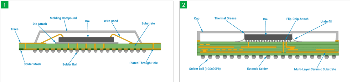
Figure (1) and Figure (2) display two examples of how BGA devices are constructed.
Figure (1) shows how the BGA die/chip is mounted on the substrate and connected to the
substrate by wire bonding technology. Figure (2) displays how the BGA die is connected
to the substrate using flip-chip technology.
The BGA die connections are routed to the solder balls using metal traces on the
substrate. BGA packages can provide more IO connections compared to dual in-line or flat
packages.
The connections from the die to the balls in BGA ICs are on average shorter than
perimeter-only type connections such as DIP ICs. Thus, leading to better performance at
high speeds.
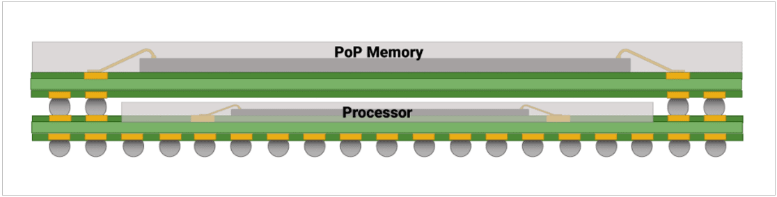
BGA PoP package
PoP is an acronym for package on package. It’s a process of stacking components or ICs
together. PoP allows multiple ICs to be integrated into a single package such as a logic
device or memory to be packaged with a processor. This greatly reduces the requirement
for PCB area and minimizes signal integrity issues on the board. Finally, it helps to
improve overall board performance at an additional cost.
 Advantages
Reducing component size
Minimizing overall cost
Reducing board complexity
Of all the packages, the BGA is the most popular package used in high I/O devices in the
industry.
Features of BGA
High lead count
No leads to bend
High interconnection density
Occupies lesser space on the board
Low inductance
Self-centering during the reflow process which reduces placement problems during surface
mount soldering
Lower thermal resistance between the package and the PCB. This allows heat generated by the
integrated circuit inside the package to flow more easily to the PCB, preventing the chip
from overheating
Learn how to breakout a .4mm BGA.
Types of BGAs
There is a wide variety of BGA device packages available in the market. Here are a few
popularly used BGAs:
Plastic over-molded BGAs (PBGAs) (Ball pitch 1.0mm, 1.27mm) – are an alternative form of the
standard BGA. These BGA incorporate a plastic-coated body, a glass-mixture laminated
substrate, and etched copper traces. PBGAs feature improved temperature stability and
preformed solder balls
High thermal metal top BGAs with low profile (HLPBGAs)
Flex Tape BGAs (TBGAs)
High thermal BGAs ( H-PBGAs)


 Quote
Quote