As electronic products continue to evolve toward higher functionality, smaller form factors, and increased integration, traditional printed circuit board architectures are rapidly approaching their physical and electrical limits. Smartphones, wearable devices, automotive ADAS modules, aerospace electronics, and high-performance computing systems all demand circuit boards capable of accommodating dense routing, fine pitch components, and multilayer interconnections without compromising reliability. Within this context, Controlled Depth Drilling has emerged not merely as a manufacturing technique, but as a foundational enabler of modern high-density PCB architectures.
In earlier generations of PCB fabrication, through-hole drilling dominated interconnection strategies. While robust and well-understood, through-holes consume valuable routing area and introduce signal integrity challenges in high-speed designs. The transition toward blind vias, buried vias, sequential lamination, and HDI (High-Density Interconnect) structures fundamentally reshaped the role of drilling. No longer is the goal simply to penetrate an entire stack-up; instead, the challenge lies in precisely terminating holes at predefined internal layers, often with tolerances measured in microns.
Controlled Depth Drilling addresses this challenge directly. By enabling drill penetration to stop at an exact depth—corresponding to a specific copper layer or dielectric boundary—it allows designers to stack more layers, shorten interconnect paths, and optimize electrical performance. From a system-level perspective, it is one of the hidden processes that quietly determine whether a high-density PCB design remains theoretical or becomes manufacturable at scale.

Controlled Depth Drilling
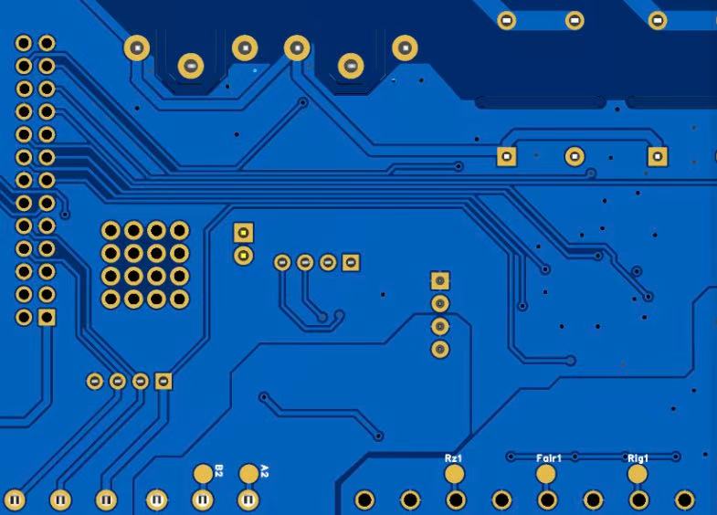
Controlled Depth Drilling refers to a precision drilling process in which the drill bit penetrates a printed circuit board to a predefined depth, stopping intentionally at a specific internal layer rather than passing completely through the board. The objective is to create structures such as blind vias, partial-depth holes, or layer-specific interconnections that are essential in high-density and multilayer PCB designs.
Unlike conventional through-hole drilling, where depth control is relatively forgiving, Controlled Depth Drilling demands accurate synchronization between mechanical motion, material properties, and real-time depth feedback. A deviation of even a few microns can result in incomplete electrical connection, internal layer damage, or catastrophic yield loss.
At its core, Controlled Depth Drilling is governed by three interdependent parameters:
Target Depth Definition – Based on the PCB stack-up, dielectric thickness, and copper layer positions
Drilling Control Mechanism – Mechanical, software-based, or sensor-assisted depth regulation
Material Response – The interaction between drill bit geometry and composite PCB materials
Only when these parameters are tightly controlled can consistent and repeatable depth accuracy be achieved across high-volume production.
Blind and buried vias are the structural backbone of high-density PCB architectures. Blind vias connect outer layers to inner layers, while buried vias interconnect internal layers without reaching the surface. Both structures allow designers to:
Reduce surface congestion
Shorten signal paths
Improve impedance control
Increase routing density
However, these benefits are only achievable when the drilling process stops exactly at the intended copper layer. Over-drilling risks cutting into underlying layers, while under-drilling leads to incomplete copper exposure and unreliable metallization.
Controlled Depth Drilling enables blind vias by guaranteeing controlled termination, ensuring that copper plating can form a reliable electrical interface during subsequent metallization steps. In multilayer HDI designs, especially those employing sequential lamination, this process becomes repetitive—each lamination cycle introduces new layers that must be drilled to different depths with absolute consistency.
From a manufacturing standpoint, this is where Controlled Depth Drilling transforms from a single operation into a core capability that determines whether a factory can support advanced HDI products at all.
Historically, early implementations of Controlled Depth Drilling relied primarily on mechanical depth stops. These systems used physical collars or preset Z-axis limits to restrict drill penetration. While effective for simple stack-ups, mechanical methods struggled with variability in board thickness, material compression, and tool wear.
Modern Controlled Depth Drilling increasingly depends on process-control-based approaches, including:
Servo-controlled Z-axis systems with micron-level resolution
Material thickness mapping prior to drilling
Dynamic depth compensation based on drill load feedback
Statistical process control (SPC) for depth consistency
In high-reliability environments—such as automotive or aerospace electronics—these advanced control mechanisms are no longer optional. They provide the stability required to maintain consistent depth across thousands of panels, despite inherent material variability.
It is tempting to view laser drilling as a replacement for Controlled Depth Drilling, particularly in microvia applications. However, the two processes serve complementary roles rather than interchangeable ones.
Laser drilling excels at extremely small diameters (typically under 150 µm) and shallow depths. Mechanical Controlled Depth Drilling, on the other hand, offers:
Greater aspect ratio capability
Superior hole wall geometry for plating
Better cost efficiency for medium-diameter blind vias
Higher throughput in volume production
In many advanced PCB designs, both technologies coexist. Mechanical Controlled Depth Drilling handles structural blind vias and controlled cavities, while laser drilling addresses ultra-fine interconnections. Understanding where one process ends and the other begins is critical for realistic DFM planning.
One of the most visible cost contributors of Controlled Depth Drilling lies in capital equipment investment. Machines capable of maintaining micron-level depth accuracy require significantly higher precision than conventional drilling systems. Enhanced servo motors, reinforced machine frames, high-speed spindles, and advanced control software all add to the initial purchase price.
Beyond acquisition, depreciation plays a long-term role. Controlled Depth Drilling machines typically experience:
Faster depreciation due to rapid technology evolution
Higher maintenance frequency to sustain depth accuracy
Increased calibration requirements
From an economic perspective, this means Controlled Depth Drilling becomes most cost-effective when utilized in high-mix, high-complexity production environments, where its capabilities are fully leveraged. For factories focused solely on low-layer-count boards, the return on investment may be difficult to justify.
Tooling cost is another significant factor. Drill bits used for Controlled Depth Drilling are subject to stricter wear limits compared to through-hole drilling. Even minor degradation in cutting edge geometry can alter penetration behavior and compromise depth accuracy.
Key tooling-related cost drivers include:
Higher-quality drill bits with advanced coatings
Reduced tool life due to conservative replacement strategies
Increased inventory management complexity
Additionally, process control itself carries cost. Continuous monitoring, SPC analysis, and frequent microsection validation require skilled labor and time. However, in my experience, these costs should be viewed as preventive investments rather than overhead. Skipping control measures often results in scrap, rework, or field failures—expenses that far exceed upfront process costs.
Yield loss is where Controlled Depth Drilling can silently erode profitability. Because blind vias are internal structures, defects are not always immediately visible. A depth error may pass initial inspection only to manifest later as:
Incomplete copper plating
Intermittent electrical opens
Reduced thermal cycling reliability
Each of these outcomes introduces hidden cost amplifiers, including extended testing time, warranty exposure, and reputational risk. For high-density PCB architectures, even a small percentage drop in yield can dramatically affect unit cost due to the already high baseline manufacturing expense.
This reality reinforces a key insight: Controlled Depth Drilling cost must be evaluated holistically, incorporating long-term reliability and customer impact—not merely per-panel processing cost.
From an electrical standpoint, Controlled Depth Drilling plays a direct role in shaping signal behavior within high-speed PCBs. Blind vias created through precise depth control reduce via stub length, which in turn minimizes signal reflections and impedance discontinuities.
Key electrical performance benefits include:
Lower insertion loss in high-frequency signals
Reduced crosstalk in dense routing environments
Improved impedance consistency
In applications such as high-speed networking or RF modules, these advantages can be decisive. Without Controlled Depth Drilling, designers are often forced to accept longer stubs or implement costly back-drilling processes as a corrective measure.
Mechanical reliability is equally influenced by Controlled Depth Drilling accuracy. A via that stops cleanly at the intended copper layer promotes uniform copper plating and stress distribution. Conversely, over-drilled or under-drilled vias may develop thin copper regions that act as crack initiation points during thermal cycling.
Controlled Depth Drilling contributes to:
Enhanced via fatigue resistance
Lower risk of barrel cracking
More consistent interlayer adhesion
In mission-critical electronics—such as automotive power control units or aerospace systems—these mechanical benefits directly translate into longer service life and reduced failure rates.
Thermal management is an increasingly important consideration in high-density PCB architectures. Blind vias and stacked via structures often serve dual roles as electrical interconnects and thermal pathways.
Controlled Depth Drilling enables designers to:
Precisely place thermal vias without damaging internal planes
Optimize copper-to-copper heat conduction paths
Avoid resin-rich via bottoms that impede heat flow
By ensuring consistent via termination, Controlled Depth Drilling supports predictable thermal performance—a factor that becomes critical as power densities continue to rise.
While the performance benefits of Controlled Depth Drilling are substantial, they are not free. Tighter depth tolerances, smaller dielectric separations, and more complex via structures all drive cost upward. The key challenge lies in balancing performance objectives with manufacturability.
In my opinion, the most successful PCB designs are those that treat Controlled Depth Drilling as a strategic optimization tool, not an indiscriminate default. When applied selectively—only where it delivers measurable electrical or thermal benefit—it yields an optimal balance between cost and performance.
| Aspect | Controlled Depth Drilling | Conventional Through-Hole Drilling |
|---|---|---|
| Drilling Objective | Stop at a specific internal layer | Penetrate entire PCB stack |
| Typical Applications | Blind vias, HDI boards, sequential lamination | Through-hole vias, low to mid-layer PCBs |
| Depth Accuracy Requirement | Micron-level control | Relatively tolerant |
| Equipment Complexity | High (servo control, depth feedback) | Moderate |
| Tooling Management | Strict wear control | Standard tool life practices |
| Impact on Signal Integrity | Reduces via stubs and reflections | Longer stubs, higher reflection risk |
| Manufacturing Cost | Higher per operation | Lower per operation |
| Suitability for High-Density PCB | Essential | Limited |
As PCB technology continues its steady evolution toward higher density, higher speed, and higher functional integration, many manufacturing processes once considered secondary have moved to the center of architectural decision-making. Controlled Depth Drilling is one of those processes. While it rarely appears in marketing materials or schematic diagrams, its influence permeates nearly every aspect of modern high-density PCB design and production.
From a purely technical standpoint, Controlled Depth-Drilling enables the realization of blind vias, buried vias, stacked via structures, and sequential lamination architectures. These features, in turn, allow designers to reduce routing congestion, shorten signal paths, and meet increasingly stringent electrical performance requirements. Without reliable depth control, many advanced PCB stack-ups would remain theoretical constructs rather than manufacturable products.
Equally important is the economic dimension. Controlled Depth-Drilling introduces higher equipment costs, stricter process control requirements, and increased tooling discipline. However, when evaluated holistically—factoring in yield stability, long-term reliability, and reduced field failure risk—its value often outweighs its cost. In high-density applications, the absence of Controlled Depth Drilling typically leads to compromises elsewhere, such as excessive via stubs, larger board sizes, or additional corrective processes.
From my perspective, the most critical insight is that Controlled Depth-Drilling should not be viewed as an isolated fabrication step. It is a design-enabling constraint, one that must be considered early in stack-up planning, material selection, and performance trade-off analysis. Organizations that integrate Controlled Depth Drilling knowledge across design and manufacturing teams consistently achieve better outcomes than those that address it reactively.
In the broader context of high-density PCB architectures, Controlled Depth Drilling represents a quiet but decisive force—one that transforms complexity into structure, and ambition into manufacturable reality.
The primary purpose of Controlled Depth-Drilling is to create holes that terminate at a predefined internal layer rather than passing through the entire board. This enables blind and buried via structures, which are essential for high-density PCB architectures, improved signal integrity, and efficient layer utilization.
Controlled Depth-Drilling improves reliability by ensuring consistent via termination, uniform copper plating, and reduced mechanical stress concentration. Accurate depth control minimizes risks such as thin copper at via bottoms, internal layer damage, and premature failure during thermal cycling.
Controlled Depth-Drilling requires higher-precision equipment, stricter process control, enhanced tooling discipline, and additional inspection steps. These factors increase upfront and operational costs, but they also reduce yield loss and long-term reliability risks in complex PCB designs.
Controlled Depth-Drilling is most critical in HDI boards, multilayer PCBs with blind or buried vias, high-speed digital designs, RF applications, and compact electronics where routing density and electrical performance are tightly constrained.
No. Controlled Depth-Drilling and laser drilling serve complementary roles. Controlled Depth Drilling is better suited for medium-diameter blind vias with higher aspect ratios and robust plating requirements, while laser drilling excels at ultra-small microvias with shallow depths. Advanced PCB designs often use both processes together.


Connect to a Jerico Multilayer PCB engineer to support your project!
Request A Quote


 Quote
Quote