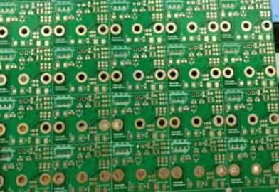
Depth Tolerance refers to the allowable deviation from a specified material removal depth or layer-termination depth during PCB fabrication. It is a quantitative measure defining how deep a tool, laser, drill, or milling operation is permitted to penetrate before exceeding acceptable limits.
More formally, Depth Tolerance can be expressed as:
Target depth (D)
Allowed deviation (+/- ΔD)
Where the acceptable deviations are often measured in microns.
Depth Tolerance may apply to:
Controlled-depth drilling (blind vias)
Laser ablation for microvias
Backdrilling to remove stubs
Milling cavities for components
Dielectric removal for embedded features
Routing features that expose internal layers
In essence, Depth Tolerance defines how accurately a manufacturing action must respect three-dimensional constraints to achieve the functional intent of the board.
A seemingly trivial deviation can lead to:
Incomplete electrical connection
Overexposed or damaged copper
Signal integrity degradation
Short circuits or leakage paths
Mechanical weakness
Failure of embedded components
Depth Tolerance is not a luxury specification; it is a fundamental reliability determinant.

Depth Tolerance
The most direct role of Depth Tolerance is to guarantee consistent electrical pathways, whether they be through-vias, blind vias, backdrilled stubs, or embedded planar structures. Excessive penetration may expose copper, cause shorts, or create irregular conductor geometries that disturb impedance. Insufficient penetration may leave dielectric material in unintended places, producing:
Higher resistive loss
Signal reflection
Impedance mismatch
Increased insertion loss
At high-frequencies, Depth Tolerance errors transition from subtle performance degradation to catastrophic system failure.
High-speed signal integrity is critically dependent on consistent via structures and controlled stub removal. A deviation of even tens of microns in backdrill depth can lead to residual via stubs that act as resonant antennas.
Effects include:
Reflection at discontinuities
Mode conversion
Radiation loss
Crosstalk coupling
Eye-diagram closure
Reduced bit-rate margins
Depth Tolerance is therefore essential to meet DDR, PCIe, SerDes, RF, and mmWave performance specifications.
Thermal conductivity in multilayer boards is shaped by both copper geometry and dielectric continuity. Poor Depth Tolerance may create uneven thermal pathways that result in localized hotspots, especially in:
Power modules
High-current vias
Thick copper boards
RF power amps
EV battery control units
Thermal gradients accelerate material fatigue, leading to:
Voiding
Delamination
Copper cracking
Dielectric breakdown
The vertical geometry of a board is a structural member. When Depth Tolerance is poorly controlled, the mechanical structure is compromised.
Examples:
Thinned substrates cause warpage
Over-cut vias weaken pad adhesion
Mis-formed cavities reduce support for components
These effects often compound through thermal cycling and vibration exposure.
Modern PCBs exhibit:
Smaller features
More layers
Thinner dielectrics
Higher frequencies
Embedded active components
These characteristics dramatically compress allowable process windows. Today, Depth Tolerance is not a secondary manufacturing concern but a first-order design constraint.
Every depth-critical process relies on equipment capability:
Drill accuracy
Laser focusing stability
Milling tool wear rate
Depth-sensing resolution
Even state-of-the-art machinery experiences drift.
A machine that is “within spec” may still produce boards that fail at scale.
PCB materials are not homogeneous.
Influencing factors include:
Resin flow variability
Glass weave undulations
Copper thickness inconsistency
Dielectric shrinkage during lamination
Organic materials introduce uncertainty that must be compensated for, not ignored.
Many depth-critical issues originate not in manufacturing, but in poorly considered design rules.
Examples:
Incorrect dielectric thickness assignment
Mis-alignment of target layers with drill depth
Impractical tolerances for the selected tools
Depth Tolerance is therefore both a design and process parameter.
Precision is expensive.
Manufacturers must constantly balance:
Reject risk
Inspection cost
Tooling investment
Cycle time
Depth Tolerance frequently becomes a negotiation between capability and affordability.
Blind vias must terminate precisely on a target layer without damaging the next layer. Excessive over-penetration risks:
Layer shorts
Copper pad failure
Microcracks
Insufficient penetration risks:
Weak metallurgical bonds
Signal loss
Intermittent via reliability
Laser via formation is powerful but inherently nonlinear due to:
Energy absorption differences
Heat-affected zones
Material reflectivity
Feedback-loop metrology is essential to prevent runaway variability.
Backdrilling removes unused via stubs to prevent resonant structures that degrade signal integrity.
Depth Tolerance determines how much stub remains:
Too shallow: inadequate mitigation
Too deep: pad damage
At >10Gbps, residual stub lengths of only 200 µm can produce measurable performance degradation.
Effective strategies include:
Controlled stack-up standardization
Avoiding unnecessary cavities
Standardizing drill depths
Designers must recognize the manufacturing system as a co-author of the PCB, not a passive executor.
Tools degrade and drift. Successful companies implement:
Hourly calibration checks
Automatic Z-axis compensation
Predictive maintenance
Manufacturing leadership is not just about machines—it is about process discipline.
Metrology is not overhead; it is insurance.
Methods include:
X-ray measurement
Ultrasonic depth mapping
Cross-section verification
SEM defect analysis
Companies with advanced inspection tend to have:
Higher first-pass yield
Lower total cost per board
Depth-Tolerance has become one of the most critical dimensions in multilayer PCB fabrication, directly influencing electrical, thermal, and mechanical performance. Its strict management is crucial to ensure the reliability of advanced, high-density, high-speed systems. As demands for thinner dielectrics, higher frequencies, and embedded architectures rise, control of Depth Tolerance transitions from optional optimization to fundamental obligation.
Depth-Tolerance in multilayer PCB fabrication represents a technical discipline that is deceptively complex, strategically significant, and increasingly central to the performance envelope of modern electronics. The vertical dimension of a PCB is no longer a passive structural parameter—it is a functional axis that determines how signals propagate, how heat dissipates, how components interact, and how long a system can operate without degradation.
In the earliest generations of printed circuit technology, tolerances were broad, materials were thick, and frequencies were low enough that microstructural deviations rarely translated into observable performance loss. Today, that landscape has vanished. The rise of HDI architectures, stacked-via configurations, RF integration, and SerDes interfaces has transformed PCBs from two-dimensional wiring platforms into compact electromagnetic ecosystems. Every micron of copper and dielectric is actively participating in a highly sensitive physical process.
From this perspective, Depth-Tolerance is not merely a manufacturing constraint—it is a physics management system. When a blind via lands too shallow, it does not simply introduce an incomplete metallurgical bond; it introduces reflection, impedance variation, and unpredictable signal behavior. When backdrilling cuts too deep, it does not simply remove copper; it damages structural integrity, introduces mechanical stress concentrations, and creates latent failure conditions. These effects are magnified by thermal cycling, humidity exposure, current density, and operating frequency, often proving fatal long after the device has passed functional test.
Yet, the challenge of Depth Tolerance is not solely technical; it is also organizational. It requires design engineers to understand manufacturing limitations, materials engineers to understand electrical performance constraints, and manufacturing engineers to balance precision with cost. Industry leaders recognize that Depth Tolerance is not solved by technology alone—it is solved by alignment of priorities, capabilities, and expectations across the development chain.
Modern production environments are moving toward more intelligent systems—adaptive drilling algorithms, material tracking, real-time depth monitoring, and predictive maintenance—and these technologies have proven effective in tightening tolerances while reducing cost. What remains difficult, however, is the cultural shift required for organizations to accept that precision is not optional, inspection is not waste, and collaboration is not inefficiency. Companies that adopt a philosophy of manufacturable design and empirical validation tend to develop products that perform better, last longer, and fail less.
At a strategic level, Depth-Tolerance also represents a market differentiator. Companies that can consistently deliver tight control over vertical geometry are able to enable architectures that competitors simply cannot fabricate. High-frequency backdrills, ultra-fine blind vias, and embedded systems are not available to organizations that view PCB fabrication as a commodity. They are built by manufacturing ecosystems willing to invest in capability—and by customers willing to value it properly.
Looking forward, the future of advanced PCBs will be defined by further miniaturization, higher frequency operation, integration of antennas, and hybrid packaging strategies that blur the lines between PCB and semiconductor domains. In this environment, Depth Tolerance will not become less important—it will become existential. Control of the Z-axis will determine whether next-generation electrical systems are feasible, manufacturable, and economically sustainable.
Ultimately, the significance of Depth Tolerance lies not in its measurement, but in its consequences. It is the hidden dimension that separates robust engineering from fragile optimism, scalable manufacturing from experimental success, and competitive advantage from operational risk. Organizations that fully comprehend this reality—technologically, organizationally, and strategically—will define the next era of electronics innovation.
How can designers reduce Depth-Tolerance risk?
By standardizing stack-ups, minimizing depth-critical features, and collaborating with skilled manufacturers early in the design cycle.
Why is Depth-Tolerance important for high-speed PCB designs?
Because small deviations alter via geometry, leading to impedance mismatch, reflection, insertion loss, and eye-diagram collapse.
Can poor Depth-Tolerance cause intermittent field failures?
Yes. Underdone or overdone features can degrade over time, especially under temperature cycling, vibration, or high current.
Which manufacturing processes require tight Depth-Tolerance?
Blind via drilling, laser drilling, backdrilling, cavity formation, routing, and controlled-depth etching.
Does tighter Depth-Tolerance always increase cost?
Yes, because it requires better machinery, inspection, tooling, and yield management. However, long-term reliability often justifies the cost.
Connect to a Jerico Multilayer PCB engineer to support your project!
Request A Quote