PCB design and
manufacturing is a complex process managing thousands of components and
connections across a multi-layer board. It is of critical importance to ensure the
production yield is error-free and one way to improve fabrication yields is to perform a
design rule check (DRC).
Catching an error in the design phase will prevent a product from being scrapped due to
power ground shorts, misaligned vias, and missing pins. DRC for manufacturing is
important in ensuring the quality of PCBs fabricated on the production line.
What is design rule check (DRC) in PCB design?
A design rule check is a set of rules used by a designer to ensure the schematic matches
all manufacturing considerations and dimensional tolerances set for a board.
Production processes have a margin of error for the variation in the products that are
manufactured. Such variations in production yield are adjusted in the design phase
itself.
What is DRC and LVS check?
A DRC allows one to verify the schematic and layout with regard to the margin of error
you can incorporate in your design. As it allows one to check if a specific board layout
correlates with the original circuit diagram or schematic of the design, it is also
called layout versus schematic (LVS) check.
What are DRC errors?
DFM stands for design for manufacturing, which is the layout topology in a way that
avoids all the problems that could be encountered during the PCB fabrication and
assembly processes.
Signal checks
The first checklist we like to implement after receiving Gerber files is signal checks. This
checklist holds key parameters that include conductor width, spacing requirements, hole
registration, and many more.
 The first checklist we like to implement after receiving Gerber files is signal
checks. This checklist holds key parameters that include conductor width, spacing
requirements, hole registration, and many more.
The first checklist we like to implement after receiving Gerber files is signal
checks. This checklist holds key parameters that include conductor width, spacing
requirements, hole registration, and many more.
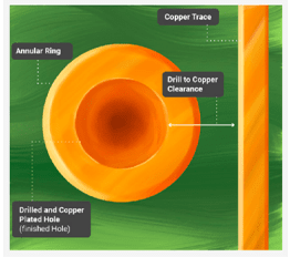
Coming to solder mask clearance, we can typically define it as a general isolation
recommendation alongside specific details characterized by the kind of surface element(s)
being isolated. Particular specifications apply to pads, which may be solder mask defined or
non-solder mask defined, and drill holes, which may be plate through-holes or non-plated
through-holes.
Silkscreen checks
Silkscreen to mask spacing, silkscreen to copper spacing, and silkscreen to hole spacing and
route spacing
DFA rules
DFA is the process of designing a device or a PCB by considering the ease of assembly as one
of the key criteria. Here are a few DFA guidelines:
Select readily available components and validate their production. This will prevent
production delays.
Apply component spacing guidelines. The component placement will determine whether the board
can be assembled, the soldering techniques and the type of thermal dissipation to be used.
Use component manufacturer recommendation for footprints. This will prevent pad mismatch
while ensuring accurate markings for identification are present.
Apply board edge guidelines. Board shape and component placement can impact panelization.
DFF stands for design for fabrication. Therefore, as the name suggests, this addresses
the issues related to fabrication. DFA stands for design for assembly. In most cases,
DFF and DFA together make up DFM.
DRC (resign rule checking) in many cases is used for DFM but is not sufficient. That’s
also acceptable to some extent because DRC issues detected in manufacturing can indeed
have a direct impact on the manufacturability of a PCB. However, DRC is different from
DFA.
DRC and DFM
DRC checks whether a problem exists or not. Like a hard pass/fail detection of a problem in
the circuit board. It ensures whether the layout connectivity precisely matches with the
schematic diagram’s defined connectivity. DRCs don’t include all the rules required to make
a bare PCB or assembled PCB. But that is only one aspect of DRC. Most commonly, DRC includes
rules that stand for defining the minimum spacing between components for the entire circuit
board or for individual layers. So, if we consider from the spacing aspect, DRC becomes a
subset of DFM, but only if the rules checked by DRC reflect a manufacturer’s requirements
for spacing. If not, DRC is solely for electrical verification.
DFF and DFA
As in most cases, DFM’s two primary components are DFF (design for fabrication) and DFA
(design for assembly). They are more involved in the nuances as compared to DRC. DRC is all
about detecting very specific deviations from the intended interconnect. On the other hand,
DFM checks PCB topology for potential manufacturing issues. Therefore, we can also say, a
DRC defect, suppose a short, will get repeated in every copy of the board, irrespective of
the quantity. Whereas it has been witnessed, if the same PCB quantity contains DFM issues,
the manifestation of problems may be seen in some circuits only.
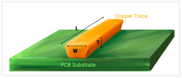
For instance, a layout that contains very thin pieces of copper can be correct if we go by
the schematic. And it will pass DRC if there is no issue with the spacing. However, the same
copper, being so thin, could form a sliver. Therefore, it could potentially detach from the
board and form solder bridges with other components during assembly. Physically, this could
happen in some PCBs and some PCBs may work as expected. So, this sort of situation can pass
DRC, but in real-world manufacturing, it can cause havoc.
DFM will detect such issues and
save manufacturers and assemblers from scrap and rework.


 Quote
Quote