


+86 13603063656
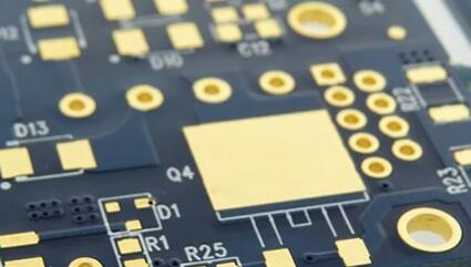
A Gold Plated PCB Board is a type of printed circuit board that incorporates a thin layer of gold on its surface, usually over nickel, to protect copper traces from oxidation and to ensure superior electrical performance. Unlike standard finishes, such as HASL (Hot Air Solder Leveling) or OSP (Organic Solderability Preservatives), gold plating provides exceptional corrosion resistance, excellent surface conductivity, and long-term reliability.
From a manufacturing standpoint, gold plating can be achieved in two primary ways:
Electroplated Gold (Hard Gold): Provides a durable and wear-resistant surface, often used for edge connectors and contact points that must withstand mechanical friction.
Electroless Nickel Immersion Gold (ENIG): A chemical process that deposits a thin layer of gold over nickel without applying current, offering flat surfaces ideal for fine-pitch components and BGA packages.
When engineers and manufacturers discuss a Gold Plated PCB Board, they are not simply highlighting aesthetics; they are referring to a solution designed for high-performance electronics where signal integrity, reliability, and resistance to environmental degradation are paramount.

Gold Plated PCB Board
The adoption of a Gold Plated PCB Board is driven by its many advantages, which extend across multiple industries—from aerospace and medical devices to consumer electronics.
Gold is an excellent conductor with very low electrical resistance. On high-frequency or high-speed PCBs, the gold surface minimizes signal loss, reduces impedance mismatches, and helps ensure clean transmission lines.
Copper oxidizes quickly when exposed to air, forming copper oxide that disrupts solderability and conductivity. Gold, being highly inert, prevents oxidation and extends the operational life of the PCB.
Unlike HASL or OSP finishes, which degrade over time, gold-plated surfaces maintain their performance over years. This makes them particularly valuable for industries where replacement is costly or even impossible—such as aerospace satellites, deep-sea equipment, or implanted medical devices.
Flat and smooth surfaces provided by ENIG make Gold Plated PCB Boards especially suitable for BGAs, QFNs, and other advanced IC packaging technologies.
While gold plating increases upfront costs, the total cost of ownership can be significantly lower in the long run. Reduced maintenance, fewer failures, and extended product lifespans translate into greater overall cost efficiency.
The perception of cost is often a barrier to wider adoption of Gold Plated PCB Boards, but a closer examination reveals their strategic value.
Durability in Harsh Environments: Devices operating in high-humidity, corrosive, or temperature-extreme environments rely on gold’s stability to remain functional.
Reduced Repair and Replacement Costs: Because of gold plating’s resistance to wear and oxidation, PCBs often outlast their alternatives, reducing the need for frequent replacements.
Signal Integrity for High-Speed Applications: As data rates continue to climb in modern electronics, reliable surface finishes become more critical, and gold plating ensures consistent electrical performance.
Brand Reputation and End-User Trust: Manufacturers that use gold-plated boards often market their products as premium, ensuring customer confidence in long-term reliability.
While beneficial, a Gold Plated PCB Board does come with some considerations:
Cost Factor: Gold is expensive, and its application increases the initial manufacturing cost of the PCB.
Risk of Black Pad Defect (ENIG-Specific): Improper plating processes may cause nickel corrosion beneath the gold, leading to solder joint failures.
Not Always Necessary: For low-cost consumer products with short life cycles, the added expense of gold plating may not be justified.
This balance between cost and long-term value is one of the reasons why manufacturers carefully evaluate whether to use ENIG, hard gold, or other alternatives depending on product requirements.
To understand the true value of gold plating, it is important to compare it against alternatives:
HASL (Hot Air Solder Leveling):
Advantages: Low cost, good solderability.
Limitations: Uneven surfaces, poor performance for fine-pitch components, limited shelf life.
Immersion Silver:
Advantages: Flat surface, good for high-frequency signals.
Limitations: Tarnishes quickly, requires special handling.
OSP (Organic Solderability Preservatives):
Advantages: Very cost-effective, environmentally friendly.
Limitations: Short shelf life, not suitable for multiple reflows or harsh conditions.
Gold Plated PCB Board:
Advantages: Long-term reliability, superior signal integrity, excellent corrosion resistance.
Limitations: Higher cost, requires careful process control.
From this comparison, it becomes clear that although a Gold Plated PCB Board is more expensive upfront, its advantages outweigh alternatives in high-reliability and long-lifespan applications.
In aerospace engineering, where failure can be catastrophic, the role of a Gold Plated PCB Board becomes indispensable.
Satellite Systems: Satellites operate in vacuum environments with extreme temperature fluctuations. Gold-plated finishes prevent oxidation, ensuring stable signal transmission even after years in orbit.
Avionics Systems: Flight control electronics demand absolute reliability. The resistance of gold-plated boards to wear and corrosion supports uninterrupted communication between subsystems.
Deep-Space Missions: In probes designed for interplanetary travel, replacing or repairing a PCB is impossible. Gold plating ensures functionality over extended mission durations.
For aerospace firms, the choice of a Gold Plated PCB Board is not about cost efficiency in the short term but about safeguarding mission-critical operations.
Medical devices represent another sector where the Gold Plated PCB Board has unique value.
Implantable Devices: Pacemakers, cochlear implants, and neurostimulators often use gold plating because it is biocompatible, preventing adverse reactions within the body.
Diagnostic Equipment: MRI machines, ultrasound devices, and CT scanners rely on gold’s signal integrity for accurate imaging.
Life-Support Systems: Reliability is paramount; gold plating minimizes the risk of PCB degradation over time, ensuring continuous function.
In my view, the role of gold plating in medical electronics highlights an ethical dimension: it is not merely about profit margins, but about protecting human life. This is why hospitals and device manufacturers willingly pay the premium for gold-plated solutions.
The digital economy runs on speed and reliability. From 5G base stations to submarine communication cables, gold plating is a crucial enabler.
5G Networks: High-frequency bands require flawless signal transmission. Gold plating supports stable impedance and low insertion loss.
Data Centers: Servers and routers must run continuously for years. Gold-plated connectors and PCBs minimize downtime and maintenance.
Subsea Cables and Repeaters: Installed at the bottom of oceans, these systems cannot be easily repaired. Gold plating extends operational lifetimes under corrosive seawater exposure.
Telecom companies have long recognized the strategic cost advantage of gold plating: although more expensive upfront, it reduces failures that would cost millions in downtime.
The automotive sector, especially with the rise of electric vehicles (EVs) and autonomous driving, is another frontier for the Gold Plated PCB Board.
Safety Systems: Airbags, anti-lock braking systems (ABS), and collision detection sensors rely on reliable circuitry that gold plating can provide.
Battery Management Systems (BMS): EV batteries demand accurate voltage monitoring. Gold’s stable conductivity ensures precise sensor readings.
Advanced Driver Assistance Systems (ADAS): Cameras, radars, and LiDAR require high-frequency signal processing, making gold plating an excellent choice for PCB finishes.
I find it particularly compelling that as cars transition from mechanical systems to rolling computers, the Gold Plated PCB Board plays a hidden yet critical role in road safety and energy efficiency.
The cost of using gold plating is often a controversial point. Let us break it down systematically:
Gold itself is expensive, with prices fluctuating based on global markets.
Specialized equipment and chemical processes add to the cost.
Thicker plating, especially for hard gold, further increases expenses.
Reduced Failures: Longer-lasting boards mean fewer replacements.
Lower Maintenance Costs: Less downtime in aerospace, telecom, or automotive industries.
Customer Satisfaction: End-users perceive products as higher quality, which strengthens brand reputation.
If a consumer device like a smartphone lasts only 2–3 years, HASL or OSP may be sufficient. But for devices expected to last a decade or more—such as aircraft electronics or medical implants—the Gold Plated PCB Board is far more cost-efficient in the long run.
This shift in perspective is crucial. Engineers and purchasing managers who evaluate only the bill of materials (BOM) may dismiss gold plating. However, when lifecycle costs are considered, the balance tips heavily in favor of gold.
As electronics evolve, so do PCB finishes. Several exciting trends are reshaping how Gold Plated PCB Boards are designed and manufactured:
Nanostructured Gold Coatings
Research is exploring ultra-thin nano-gold layers that reduce material usage while retaining performance.
These could significantly cut costs while enhancing surface properties.
Environmentally Friendly Plating Processes
Traditional plating involves hazardous chemicals. Future developments aim to reduce environmental impact through greener chemistries.
Hybrid Finishes (Selective Plating)
Instead of coating the entire board, manufacturers are developing ways to apply gold only where needed, such as connectors or pads, reducing waste.
Integration with Flexible and Rigid-Flex Boards
As wearable devices and IoT applications grow, gold plating is being optimized for flexible PCBs, which must endure constant bending.
Thinner Yet Stronger Coatings
Advanced deposition techniques like atomic layer deposition (ALD) promise stronger adhesion and better reliability at reduced thicknesses.
In my opinion, the biggest breakthrough will come from cost-reduction technologies. If the industry can deliver gold plating at significantly lower cost without sacrificing performance, adoption will expand even into mainstream consumer electronics.
A Gold Plated PCB Board is more than a surface finish—it represents the pinnacle of signal integrity, corrosion resistance, and long-term reliability in electronic design.
Technical Value: Superior conductivity, solderability, and wear resistance.
Economic Value: Higher upfront cost, but reduced lifecycle cost.
Industry Impact: Essential in aerospace, telecom, medical, AI, and quantum.
Future Outlook: Smarter, thinner, eco-friendly plating technologies.
From my perspective, the evolution of Gold Plated PCB Boards mirrors the trajectory of modern technology itself: moving toward higher performance, lower waste, and longer reliability horizons.
In an age where electronics permeate every aspect of life—from self-driving cars to medical implants to quantum processors—the Gold Plated PCB Board remains a quiet but irreplaceable backbone of progress.
1. What is the difference between rolled copper foil and electrolytic copper foil?
Rolled copper foil is produced by mechanically rolling copper into thin sheets, offering better surface quality and mechanical strength. Electrolytic copper foil is deposited via an electrolytic process and is more flexible and cost-effective.
2. Why choose a Gold Plated PCB Board over HASL or OSP?
A Gold Plated PCB Board offers superior signal integrity, better corrosion resistance, and longer shelf life compared to HASL or OSP, making it ideal for high-reliability applications.
3. What industries benefit the most from Gold Plated PCB Boards?
Industries such as aerospace, military, automotive safety systems, medical devices, and high-frequency communication equipment benefit the most due to their high performance and reliability requirements.
4. Are Gold Plated PCB Boards suitable for high-speed digital circuits?
Yes. The excellent conductivity and flatness of gold-plated surfaces reduce signal loss and impedance mismatches, making them suitable for high-speed and high-frequency circuits.
5. How does plating thickness affect Gold Plated PCB Board performance?
Thicker gold layers improve durability and wear resistance, particularly for contact points. However, excessive thickness may increase cost without proportional performance gains. Optimal thickness is determined by the application’s specific requirements.


Connect to a Jerico Multilayer PCB engineer to support your project!
Request A Quote


 Quote
Quote