High density interconnect PCBs are a way of making more room on your PCB to
make them more efficient and allow for faster transmission. It’s relatively easy for
most enterprising companies that are using printed circuit boards to see how this can
benefit them.
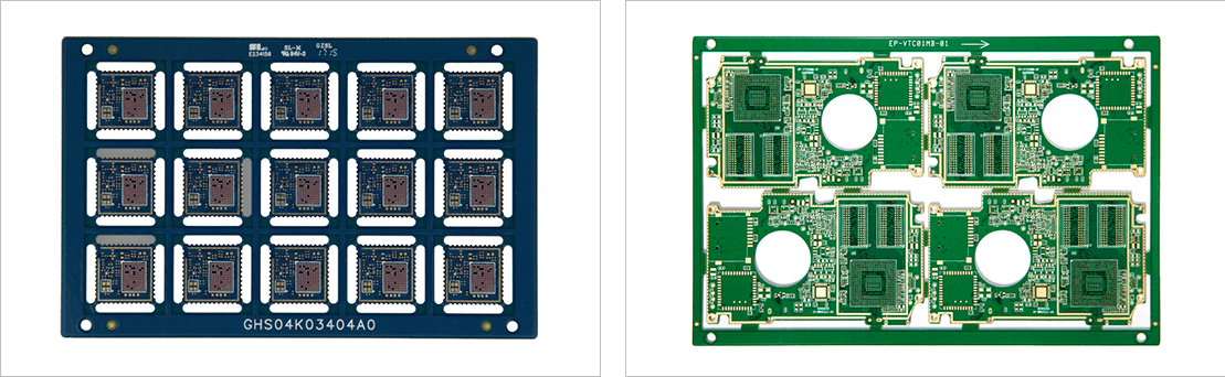
High density interconnect (HDI) PCBs represent one of the fastest-growing segments of
the PCB market. Because of its higher circuitry density, the HDI technology can
incorporate finer lines and spaces, smaller vias and capture pads, and higher connection
pad densities. A high-density PCB features blind and buried vias and often contains
microvias that are .006 in diameter or even less.
Key HDI PCB Benefits
The evolution of PCB HDI technology has given engineers greater design
freedom and flexibility than ever before. Designers using HDI high density interconnect
methods now can place more components on both sides of the raw PCB if desired. In
essence, an HDI PCB gives designers more space to work with, while allowing them to
place smaller components even closer together. This means that a high-density
interconnect PCB ultimately results in faster signal transmission along with enhanced
signal quality.
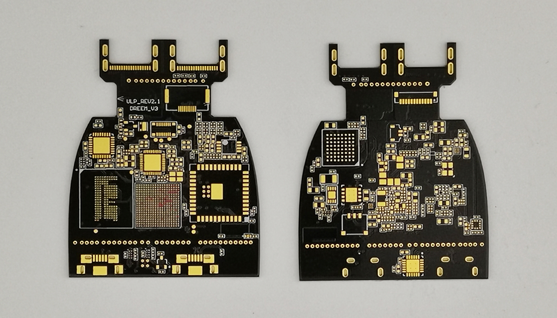
HDI PCB is widely used to reduce the weight and overall dimensions of products, as well
as to enhance the electrical performance of the device. The high-density PCB is
regularly found in mobile phones, touch-screen devices, laptop computers, digital
cameras and 4G network communications. The HDI PCB is also prominently featured in
medical devices, as well as various electronic aircraft parts and components. The
possibilities for high-density interconnect PCB technology seem almost limitless.
HDI PCB Applications
HDI boards are appropriate for a wide range of industries. As mentioned above, you’ll find them in all types of digital devices, like smartphones and tablets, where miniaturization is key to the effective application of the product. You can also find high-density interconnect PCBs in automobiles, aircraft and other vehicles that rely on electronics.
One of the most critical areas where the high-density PCB is making huge inroads is in the medical arena. Medical devices frequently need small packages with high transmission rates that only HDI PCBs can supply. For example, an implant needs to be small enough to fit in the human body, but any electronics involved in that implant absolutely must efficiently allow for high-speed signal transmission. Here, the HDI PCB indeed is a godsend. HDI PCBs can also be useful in other medical equipment, like emergency room monitors, CT scans and much more.


 Quote
Quote