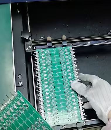
High-speed digital and RF systems have pushed printed circuit board (PCB) performance into regimes where signal integrity is critical. Among the most persistent challenges designers face is Impedance Discontinuity, which refers to any deviation of the characteristic impedance along a signal path. These deviations act as “speed bumps” for high-frequency signals, causing reflections, distortions, and potential data loss.
Modern PCBs carry signals well into the gigahertz range, where the physical geometry of copper traces, the properties of dielectric materials, and even minor manufacturing tolerances significantly influence impedance. In earlier generations of electronics, small changes in impedance were often tolerated without major consequences. Today, however, even a few ohms of impedance mismatch can result in unacceptable jitter, degraded eye diagrams, or increased bit error rates.

Impedance discontinuity
When a signal encounters a discontinuity—such as a via stub, an abrupt trace width change, or a connector with mismatched impedance—part of the signal’s energy is reflected back toward the source. This reflection reduces the amplitude of the forward-traveling wave and introduces timing uncertainty. In differential signaling, asymmetrical discontinuities can lead to mode conversion, increasing electromagnetic interference (EMI) and reducing noise immunity.
Trace geometry: Sudden width changes, neck-down areas, or routing transitions.
Layer stack-up: Variations in dielectric thickness or permittivity between layers.
Vias and connectors: Stubs, pads, and pin fields introduce parasitic capacitance and inductance.
Manufacturing tolerances: Etching accuracy, copper plating thickness, and solder mask variations.
Rather than being a mere nuisance, Impedance Discontinuity directly affects high-speed data integrity. For example, in DDR5 memory interfaces or 112 Gbps PAM4 SerDes links, maintaining strict impedance control throughout the path is non-negotiable. Designers must approach impedance not as a single value but as a system-level parameter requiring continuity and consistency.
In the context of high-speed PCB design, Impedance Discontinuity describes any abrupt deviation from the characteristic impedance along a transmission path. The characteristic impedance, often denoted Z0Z_0, is determined by the trace geometry, dielectric material, and proximity to reference planes. When a signal moves through a uniform medium with consistent parameters, it experiences no reflection. The moment the impedance shifts — because of a trace-width change, a via transition, or a connector pin — part of the signal reflects back, leading to degraded performance.
This concept is not abstract. It can be quantified with transmission-line theory and confirmed through time-domain reflectometry (TDR). Designers often specify “±10%” as a rule of thumb for impedance variation, but for very high data rates, the tolerance window can shrink to ±5% or less.
Trace Width and Thickness
A sudden change in trace width directly alters impedance. For example, a 50-Ω trace necked down to 40 Ω for a via escape can cause localized reflection.
Dielectric Constant (Dk)
PCB laminates exhibit different Dk values depending on frequency, resin content, and glass weave orientation. If a trace transitions from one dielectric region to another (e.g., from prepreg to core), impedance discontinuity occurs.
Copper Surface Roughness
High-frequency signals see more of the copper surface texture. Variations in roughness can slightly increase effective impedance and insertion loss.
Reference Plane Consistency
When a trace switches reference planes (for example from ground to power plane), the return current path shifts, changing the inductive and capacitive environment.
Vias and Pads
Vias add parasitic inductance and capacitance. A via stub behaves as a resonant element at certain frequencies, creating strong reflections. Backdrilling or controlled depth drilling can minimize these stubs.
Designers frequently use a combination of 2D field solvers, 3D EM simulation, and circuit-level models. A discontinuity is modeled as a localized impedance bump or dip, which can be represented by a small network of lumped L and C elements. In system-level simulation, these discontinuities are embedded within IBIS-AMI or SPICE models to predict their effect on eye diagrams.
For single-ended signals, discontinuity simply reflects energy. For differential pairs, an additional phenomenon arises: mode conversion between differential and common modes. This leads to radiated EMI and susceptibility to noise. Designers must ensure that both lines in a differential pair maintain equal geometry and environment throughout their run.
Signal integrity (SI) encompasses all the parameters that define how faithfully a signal travels from source to destination. Impedance Discontinuity is among the most common SI pitfalls. In essence:
Reflections: Each discontinuity reflects part of the signal back.
Timing Distortion: Multiple reflections cause ringing and timing jitter.
Increased Crosstalk: Mode conversion can make a system more prone to interference.
Loss of Bandwidth: High-frequency content of signals suffers first, distorting rise times.
Digital systems once ran at tens of MHz; now they routinely exceed 10 GHz effective edge rates. At these speeds, even a 0.5-mm stub or a 2-Ω impedance bump can create a noticeable discontinuity. Consequently, high-speed PCBs require precise control of every transition.
TDR injects a fast step signal into a trace and measures reflections. A perfect 50-Ω line shows a flat response; a discontinuity appears as a bump (impedance increase) or dip (impedance decrease). TDR is invaluable during prototype validation to identify where impedance discontinuities occur.
In the frequency domain, S-parameters such as S11 (return loss) quantify how much signal reflects from a discontinuity. Designers use S-parameter sweeps to ensure their channels meet loss and return-loss specifications across frequency.
At very high speeds, even small differences in laminate properties can produce measurable impedance shifts. Impedance Discontinuity can be aggravated or alleviated depending on how well the material parameters stay consistent across the PCB stack-up. The key material parameters are:
Dielectric Constant (Dk): Determines the speed of signal propagation and effective capacitance per unit length.
Dissipation Factor (Df): Influences insertion loss but also interacts with impedance stability at high frequency.
Glass Weave Effect: Uneven fiberglass bundles can locally shift Dk and cause micro-discontinuities.
FR-4: Ubiquitous but relatively high variation in Dk and Df. Good for moderate speeds but can make impedance matching harder beyond 6 GHz edge rates.
Low-Loss Laminates (e.g., Megtron 6, Isola Tachyon): Offer tighter Dk tolerances, better high-frequency stability, and more predictable impedance.
Hybrid Stack-Ups: Using low-loss cores for critical layers and FR-4 for others can control cost but must be modeled carefully to prevent discontinuities where different materials meet.
Glass cloth can introduce small periodic variations in dielectric constant. For differential pairs, this can result in skew. Skew translates into mode conversion and therefore discontinuity. Designers may:
Use spread glass styles.
Route traces at small angles to glass weave.
Specify tighter material tolerances with the manufacturer.
When a signal changes its reference plane from ground to power or from one ground plane to another, its return current path shifts. This shift modifies the inductive and capacitive coupling, producing an Impedance Discontinuity. The usual mitigation is to place stitching vias or capacitors to provide a low-impedance return path.
Crossing a split plane without a return path is one of the most severe discontinuities. Always provide a bridging capacitor or adjust routing to avoid crossing plane gaps.
Specify precise prepreg and core thicknesses. Work with the fabricator to lock down stack-up early in the design process.
Use symmetrical stack-ups to ensure uniform mechanical behavior and predictable impedance.
Using thin dielectrics between power and ground can also reduce loop inductance, indirectly improving impedance continuity.
Backdrilling removes unused via stubs but you can go further:
Tapered Drills: Gradually changing via barrel diameter reduces abrupt impedance changes.
Embedded Capacitance Pads: Intentionally adding small capacitive pads to balance inductance and capacitance.
Non-Plated Through Holes (NPTH) as Ground Returns: Surrounding signal vias with dedicated ground vias to confine the return current.
These techniques make Impedance Discontinuity predictable rather than random, enabling designers to fine-tune channel performance.
At very high data rates, the way a trace transitions to an SMA or coaxial connector can create a major discontinuity. Edge-launch connectors minimize the transition region. Careful pad design, ground via fences, and the use of launch models from connector vendors help keep impedance consistent.
Signal traces do not exist in isolation. Mutual coupling between adjacent traces can either aggravate or mask discontinuities. By controlling spacing and stack-up, you can simultaneously minimize crosstalk and keep impedance steady. Small, intentional guard traces or ground fills may also help.
High-speed PCB designers must consider the chip package as part of the channel. The package breakout region can have very different impedance than the on-board traces. Request S-parameter or IBIS-AMI models from your IC vendor to include this region in your analysis.
If the PCB connects to cables or backplanes, the impedance continuity must extend beyond the board edge. The connector and cable must be specified for the same impedance target. For example, a 100-Ω differential pair on the PCB should transition into a 100-Ω twisted-pair cable with minimal geometric change.
Sometimes thermal relief pads, copper thieving, or mechanical mounting holes impose abrupt changes to copper density. These can slightly affect local impedance. You may need to simulate these areas or negotiate changes with the mechanical team to avoid hot spots of Impedance Discontinuity.
For extremely high frequencies, VNAs measuring up to 50 GHz or more give a full picture of return loss (S11) and insertion loss (S21). This confirms how discontinuities behave across the band.
After the board is assembled, measure the eye diagram at the receiver. Any Impedance Discontinuity large enough to cause reflections will close the eye at certain data rates. This gives an end-to-end, system-level confirmation.
If your application is serial data links, BERT testing shows real-world performance. Reducing impedance discontinuities typically lowers BER significantly.
Many discontinuities originate from process variation rather than design intent. Communicate:
Controlled Impedance Requirements: Specify target impedance and tolerance explicitly.
Test Coupons: Ask the fabricator to include them and report TDR results.
Plating Control: Copper thickness can vary; tighter control yields more predictable impedance.
Stack-Up Lockdown: Do not leave prepreg or core thickness “as per availability.” Fix them in the build note.
The path to reliable high-speed PCBs lies in recognizing and mitigating Impedance Discontinuity at every step — from stack-up design to trace routing, via structures, and connectors. With gigahertz signals, nothing is “too small” to matter. Through careful material selection, simulation, prototyping, and collaboration with expert fabricators like JM PCB, engineers can deliver designs that meet today’s stringent signal integrity requirements.
The techniques described above form a layered defense:
Design Right: Start with consistent stack-ups and trace geometries.
Simulate Early: Use field solvers and 3D EM models to foresee trouble spots.
Build Smart: Partner with fabricators who understand controlled impedance.
Verify Thoroughly: Use TDR, S-parameters, and eye diagrams to confirm real-world performance.
By systematically applying these practices, you reduce risk, improve product reliability, and achieve faster time to market.
1. Does solder mask affect impedance?
Yes. Solder mask slightly increases the effective dielectric constant, lowering impedance. Thicker mask or mask openings can introduce minor discontinuities.
2. How does glass weave affect impedance discontinuity?
The glass weave in PCB laminates can cause local Dk variation, leading to skew in differential pairs and subtle impedance shifts. Using spread glass or routing traces at slight angles can mitigate this.
3. Can via backdrilling completely eliminate impedance discontinuity?
Backdrilling greatly reduces the discontinuity caused by via stubs but does not completely remove parasitics. Careful modeling is still advised.
4. Is differential impedance more sensitive to discontinuity than single-ended impedance?
Yes. Differential signaling relies on symmetry; any imbalance can convert differential energy into common mode, increasing EMI and reducing noise immunity.
5. How can a fabricator help me maintain impedance targets?
Good fabricators provide controlled impedance services, test coupons, and engineering feedback on stack-ups. Collaborating early with your manufacturer — such as JM PCB — ensures your impedance targets are realistic and manufacturable.
Connect to a Jerico Multilayer PCB engineer to support your project!
Request A Quote