


+86 13603063656
The electronics industry has entered a phase where interconnect density, not transistor scaling, defines system capability. As semiconductor nodes advance toward physical and economic limits, the responsibility for performance, power efficiency, and reliability increasingly shifts from silicon to substrate-level engineering.
Ultra-High Density Interconnect (Ultra-HDI) is no longer a niche solution reserved for smartphones or wearable devices. It has become a structural requirement for AI accelerators, advanced packaging, automotive electronics, medical devices, and aerospace systems. At the heart of this transformation lies a deceptively small but fundamentally disruptive technology: Laser-Drilled Microvia.
Laser-Drilled Microvia technology represents more than a manufacturing upgrade. It signals a paradigm shift in how engineers think about vertical interconnection, layer utilization, and system-level optimization. What once was a mechanical constraint has now become a design variable—and with it comes both opportunity and responsibility.

Laser-Drilled Microvia
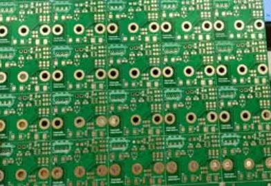
A Laser-Drilled Microvia is a small-diameter vertical interconnect created by laser ablation to electrically connect adjacent layers within a multilayer PCB or substrate. Unlike mechanically drilled vias, which typically exceed 150 µm in diameter, microvias usually range from 30 µm to 100 µm, with depths tightly controlled to one dielectric layer.
What distinguishes Laser-Drilled Microvia technology is precision, selectivity, and scalability:
Precision: Laser energy can be focused with micron-level accuracy
Selectivity: Specific dielectric materials can be removed without damaging copper targets
Scalability: Millions of microvias can be formed in a single panel with consistent geometry
From an engineering standpoint, a Laser-Drilled-Microvia is not merely a smaller via—it is a fundamentally different interconnect structure. Its shallow depth, reduced barrel volume, and controlled geometry drastically alter electrical, thermal, and mechanical behavior.
Key defining attributes include:
Typically blind (L1–L2, L2–L3, etc.)
Low aspect ratio (often ≤1:1)
Copper-filled or copper-plated
Designed for sequential lamination processes
These attributes make Laser-Drilled-Microvia structures uniquely suited for high-density routing and advanced packaging, where every micron of real estate matters.
The transition from mechanical drilling to Laser-Drilled -technology did not occur overnight. It was driven by compounding constraints rather than a single breakthrough.
Mechanical drilling reached practical limits due to:
Drill bit wear and breakage
Registration inaccuracies at small diameters
Excessive stub lengths
Increasing panel thickness variability
Laser drilling emerged as the only viable solution once interconnect density crossed a critical threshold. Initially adopted in HDI consumer electronics, Laser-Drilled Microvia processes rapidly matured through automotive qualification, aerospace reliability testing, and high-volume manufacturing demands.
my experience, the most profound shift was not technical—it was philosophical. Designers stopped asking “How small can we drill?” and began asking “How efficiently can we connect layers?” That shift unlocked entirely new routing strategies.
The advantages of Laser-Drilled-Microvia technology extend far beyond size reduction. When properly implemented, they redefine PCB performance at multiple levels.
Laser-Drilled-Microvia structures reduce:
Parasitic inductance
Via stub resonance
Return path discontinuities
This directly improves signal integrity, especially in multi-gigabit and millimeter-wave applications.
By enabling via-in-pad and stacked configurations, Laser-Drilled Microvia technology:
Maximizes routing channels
Shortens trace lengths
Enables finer pitch components
This is why leading fabricators such as JM PCB increasingly position Laser-Drilled Microvia capability as a core competency rather than an optional service.
Shorter vias experience:
Lower thermal expansion stress
Reduced copper fatigue
Improved CAF resistance
From a lifecycle perspective, Laser-Drilled Microvia adoption often improves field reliability, even as density increases.
Implementing Laser-Drilled Microvia technology successfully requires tight process control across multiple domains:
Laser wavelength optimization
Dielectric absorption tuning
Plasma desmear integration
Copper plating uniformity
Manufacturers with deep HDI experience—such as JM PCB—understand that Laser-Drilled Microvia yield is not determined by drilling alone, but by system-level process integration.
This is where many projects succeed or fail. Laser drilling may be precise, but without proper metallization and inspection, microvias can become latent failure points.
As data rates climb into multi-gigabit and millimeter-wave regimes, interconnect behavior becomes a dominant factor in system performance.
Laser-Drilled Microvia structures improve signal integrity by:
Reducing via stubs
Minimizing impedance discontinuities
Supporting controlled return paths
Compared to mechanically drilled vias, microvias behave more like short transmission segments than lumped parasitic elements.
From a power delivery perspective, Laser-Drilled Microvia technology enables:
Lower inductance power distribution networks
Closer placement of decoupling capacitors
Reduced ground bounce
In my view, one of the most underappreciated benefits of Laser-Drilled Microvia adoption is its impact on power integrity, which often dictates system stability more than signal routing itself.
The interaction between Laser-Drilled Microvia structures and surrounding materials determines both performance and durability.
Laser drilling relies on controlled ablation of dielectric materials. Material selection therefore directly influences:
Via wall smoothness
Ablation consistency
Copper adhesion quality
Low-loss dielectrics used in high-speed designs must be carefully matched with laser parameters to avoid thermal damage or residue formation.
Copper plating within Laser-Drilled Microvia structures must achieve:
Void-free fill
Uniform grain structure
Strong interfacial bonding
Poor copper fill does not always fail immediately—it often manifests as latent reliability degradation, making process discipline essential.
| Performance Area | Impact of Laser-Drilled Microvia |
|---|---|
| Signal Integrity | Reduced reflections and impedance discontinuities |
| Power Integrity | Lower loop inductance and improved decoupling |
| Thermal Reliability | Reduced stress concentration |
| Board Size | Enables miniaturization |
| Layer Utilization | More efficient vertical routing |
As electronic systems push toward ever-higher levels of integration, performance, and functional density, Ultra-HDI is no longer a forward-looking concept—it is a present-day necessity. Within this context, Laser-Drilled Microvia technology stands as a foundational enabler rather than a supporting feature.
What becomes clear through technical analysis and manufacturing practice is that Laser-Drilled Microvia structures redefine how engineers approach vertical connectivity. They compress electrical distance, reduce parasitic behavior, and unlock routing strategies that are simply impossible with conventional drilling methods. In advanced packaging environments—where signal integrity, power delivery, and thermal behavior are tightly interwoven—these advantages compound at the system level.
From an engineering perspective, the real power of Laser-Drilled Microvia technology lies in its predictability. When geometry, materials, and process windows are properly controlled, microvias behave as reliable, repeatable interconnect elements. This predictability allows designers to move away from conservative over-design and toward intentional optimization, improving performance while managing cost and risk.
Equally important is the manufacturing ecosystem that supports this technology. Fabricators with mature HDI capabilities understand that Laser-Drilled Microvia success depends on end-to-end integration—from laser ablation and desmear chemistry to copper metallization and inspection. In this sense, Ultra-HDI is as much a manufacturing discipline as it is a design methodology.
Looking forward, Laser-Drilled Microvia technology will continue to evolve alongside advanced packaging, AI computing, and heterogeneous integration. Diameters will shrink, alignment tolerances will tighten, and reliability expectations will rise. Yet the core principle will remain unchanged: system performance increasingly depends on how efficiently layers communicate, not how fast transistors switch.
In conclusion, Laser-Drilled Microvia technology is not simply unlocking Ultra-HDI—it is defining its boundaries, possibilities, and future trajectory.
1. Is Laser-Drilled Microvia technology necessary for all PCB designs?
No. It is most beneficial for high-density, high-speed, or advanced packaging applications. Simpler designs may still rely effectively on traditional via technologies.
2. Why are Laser-Drilled Microvia structures preferred over mechanical vias in Ultra-HDI designs?
Laser-Drilled Microvia structures offer smaller diameters, lower parasitic effects, and greater routing flexibility, making them essential for high-density and high-speed PCB designs.
3. Are stacked Laser-Drilled Microvia structures reliable?
They can be reliable when properly designed and manufactured, but stacked configurations introduce higher stress concentration. Staggered designs are often preferred for long-term reliability.
4. How does Laser-Drilled Microvia technology improve signal integrity?
By reducing via stubs and minimizing impedance discontinuities, Laser-Drilled Microvia structures support cleaner signal transitions and higher data rates.
5. What role does copper filling play in Laser-Drilled Microvia reliability?
Copper-filled microvias improve mechanical strength, reduce thermal fatigue, and enhance electrical performance compared to hollow plated structures.


Connect to a Jerico Multilayer PCB engineer to support your project!
Request A Quote


 Quote
Quote