


+86 13603063656
In the ever-evolving electronics industry, dense PCB Multilayer Boards have become the cornerstone of advanced electronic devices. These boards, composed of multiple layers of conductive copper and insulating material, allow for highly complex circuits in a compact footprint. Unlike single or double-layer boards, Multilayer Boards can incorporate intricate routing, power distribution networks, and signal integrity optimization, all within a limited physical space.
The fundamental structure of a Multilayer Board involves alternating layers of conductive copper and insulating substrates. Standard fabrication materials include FR-4 for general applications and high-performance laminates such as Rogers or polyimide for high-frequency or thermal-sensitive applications. The layers are interconnected via plated through-holes (PTHs) or blind/buried vias, which ensure electrical continuity across the board.

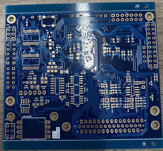
multilayer board
Compactness and Space Efficiency: By stacking multiple circuit layers vertically, designers can fit more functionality into smaller boards, crucial for modern smartphones, wearables, and medical electronics.
Improved Signal Integrity: The dedicated power and ground planes within Multilayer Boards reduce electromagnetic interference (EMI) and crosstalk, ensuring reliable high-speed signal transmission.
Enhanced Thermal Management: Strategically designed layers help dissipate heat more effectively, preventing hotspots in high-power applications.
Higher Reliability and Durability: Multilayer construction provides mechanical stability and reduces the likelihood of signal degradation over time.
While Multilayer Boards provide unmatched benefits, designing them is inherently complex:
Layer Alignment: Maintaining precise registration across multiple layers is critical to avoid short circuits or open traces.
Via Management: Blind, buried, and microvias must be carefully planned to avoid congestion and maintain electrical performance.
Signal Routing: High-speed or high-frequency signals require controlled impedance traces and proper isolation, increasing design complexity.
Fabrication Limitations: The more layers included, the stricter the tolerance requirements, increasing production difficulty and cost.
The next step in mastering dense Multilayer Boards is understanding the design methodologies that tackle their complexity:
An optimal layer stackup minimizes EMI, reduces signal reflections, and simplifies routing. Designers often use simulation tools to determine the most effective sequence of signal, power, and ground layers.
To ensure signal integrity in dense Multilayer Boards, differential pair routing, controlled impedance traces, and via stitching are essential. These techniques prevent timing errors and signal degradation in high-frequency circuits.
Thermal vias, copper balancing, and material selection are critical. High-density multilayer boards tend to trap heat, which can lead to component failure if not managed properly.
To conquer the inherent complexity, DFM guidelines must be followed. This includes via aspect ratio management, trace width tolerance, and copper weight considerations.
As the density of a Multilayer Board increases, maintaining signal integrity becomes a critical challenge. High-speed circuits are sensitive to impedance mismatches, crosstalk, and electromagnetic interference. Designers implement several strategies to mitigate these issues:
Differential pairs are used for high-speed signals to reduce noise and electromagnetic emissions. In Multilayer Boards, differential pair routing must consider trace width, spacing, and the proximity to ground planes to maintain controlled impedance.
Maintaining impedance within strict tolerances ensures signal integrity across high-frequency traces. Layer stackup planning and dielectric material selection directly influence impedance performance.
Strategically placed vias connect ground planes and provide return paths for high-speed signals, reducing EMI and signal degradation. Via placement must be optimized to avoid introducing additional parasitic inductance or capacitance.
Recommendation: For complex high-speed Multilayer Boards, JM PCB offers advanced routing and via fabrication services to ensure that signal integrity is maintained across multiple layers, even in dense designs.
Thermal issues are a major concern in dense Multilayer Boards, particularly in high-power applications. Without proper heat dissipation, components can overheat, leading to performance degradation or failure.
Thermal vias transfer heat from internal layers to external copper planes or heat sinks. Their placement and diameter are crucial in managing board temperature.
Uneven copper distribution can cause warping during fabrication. Proper copper balancing ensures mechanical stability and consistent thermal performance.
For applications requiring high power handling, materials with enhanced thermal conductivity, such as metal-core PCBs or thermally enhanced laminates, can be integrated into multilayer designs.
Designing for manufacturability is essential to ensure that the theoretical design translates effectively into a real, functional PCB. Key considerations include:
Via Aspect Ratio: The ratio of board thickness to via diameter must remain within fabrication capabilities. Extremely high aspect ratios may require laser-drilled microvias.
Trace Width and Spacing: Narrow traces in dense boards must adhere to fabrication tolerances to prevent shorts or opens.
Panelization: Proper panel design can reduce material waste and simplify assembly processes.
Dense Multilayer Boards must withstand mechanical stress, thermal cycling, and long-term usage. Key factors include:
Board Warpage: Minimizing warpage ensures proper component placement and solder joint reliability.
Via and Pad Integrity: Blind, buried, and through-hole vias must maintain electrical continuity and withstand thermal stress.
Layer Adhesion: Strong lamination prevents delamination, a common failure mode in high-layer-count boards.
Passive components such as resistors and capacitors are increasingly embedded within Multilayer Boards, freeing surface space and improving performance.
Emerging techniques allow for direct printing of conductive traces, opening new possibilities for non-planar multilayer structures.
Low-loss dielectrics and hybrid stackups improve signal transmission at GHz frequencies.
AI-assisted routing and stackup planning reduce design time and error rates, essential for conquering complexity in Multilayer Boards.
With increasing regulatory pressure, designers and manufacturers must also consider environmental impact:
Use of lead-free finishes such as ENIG or immersion silver.
Implementation of halogen-free laminates.
Recycling processes for copper and fiberglass waste.
Dense Multilayer Boards represent the pinnacle of PCB engineering, combining high functionality, miniaturization, and reliability. By leveraging advanced design methods, rigorous testing, and trusted manufacturing partners, designers can successfully conquer complexity and deliver high-performance products to market.
Key takeaways:
Multilayer-Boards enable unprecedented circuit density and performance but require meticulous planning.
Advanced methods—controlled impedance, thermal via arrays, embedded components—are essential to meeting next-generation demands.
Collaborating with proven manufacturers like JM PCB ensures the transition from concept to production is smooth and reliable.
As technology advances, the ability to innovate within the constraints of physical space and materials will define the future of Multilayer-Boards, driving progress across every industry from consumer electronics to aerospace.
What is the difference between rolled copper foil and electrolytic copper foil?
Rolled copper foil is produced by mechanically rolling copper into thin sheets, offering better surface quality and mechanical strength. Electrolytic copper foil is deposited via an electrolytic process and is more flexible and cost-effective.
Why are blind and buried vias used in Multilayer-Boards?
Blind vias connect outer layers to inner layers without passing through the entire board, while buried vias connect only inner layers. This allows more routing flexibility and conserves space for complex designs.
How many layers can a Multilayer-Board have?
Multilayer Boards typically range from 4 to 32 layers, but advanced applications can go beyond this with specialized fabrication techniques.
What materials are recommended for high-frequency Multilayer-Boards?
Materials like Rogers, Teflon-based laminates, or polyimide are preferred for high-speed applications due to their low dielectric constant and stable thermal properties.
How does layer stackup affect signal integrity?
Proper stackup reduces crosstalk, minimizes EMI, and ensures controlled impedance, which is critical for high-speed digital and RF circuits.


Connect to a Jerico Multilayer PCB engineer to support your project!
Request A Quote


 Quote
Quote