


+86 13603063656
The term Package Types refers to the physical and structural configurations used to encapsulate and connect semiconductor dies to printed circuit boards. In the context of BGA technology, these types determine not only how electrical connections are distributed but also how mechanical and thermal stresses are managed throughout the assembly process.
At its core, a package serves three primary functions: it protects the silicon die, provides electrical interconnection between the die and the PCB, and dissipates heat efficiently. The Package Types in BGA systems are categorized by several design variables — ball pitch, substrate materials, layer count, and interposer structure. Each factor plays a critical role in defining the overall performance envelope.
| Category | Description |
|---|---|
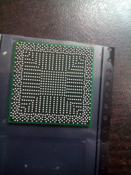
| Full Name | Ball Grid Array (BGA) |
| Definition | A type of surface-mount packaging where solder balls are arranged in a grid pattern on the bottom of the package to provide electrical connection between the IC and the PCB. |
| Structure | Consists of a silicon die mounted on a substrate, with solder balls attached underneath for interconnection to the PCB. |
| Key Advantage | Higher pin density and improved electrical performance compared to leaded packages. |
| Thermal Performance | Excellent heat dissipation due to shorter interconnection paths and larger contact area. |
| Electrical Performance | Reduced signal inductance and crosstalk, making it ideal for high-speed circuits. |
| Mechanical Strength | Stronger joint reliability due to distributed stress through multiple solder balls. |
| Inspection Difficulty | Harder to inspect visually; requires X-ray inspection for solder joint validation. |
| Rework Difficulty | Reballing and reflow processes are complex and require precise temperature control. |
| Applications | Widely used in CPUs, GPUs, FPGAs, memory modules, and high-performance embedded systems. |
| Common Types | PBGA (Plastic BGA), CBGA (Ceramic BGA), TBGA (Tape BGA), and MicroBGA. |
| Typical Pitch Sizes | 0.3 mm to 1.0 mm (smaller for fine-pitch designs). |
| Advantages Summary | Compact design, excellent electrical and thermal performance, high I/O density. |
| Disadvantages Summary | Costlier rework, inspection complexity, and potential warpage during reflow. |
For example, plastic over-mold BGAs are commonly used in cost-sensitive consumer devices because they are inexpensive and reliable for moderate thermal loads. Conversely, ceramic BGAs are designed for aerospace and high-performance computing due to their excellent mechanical rigidity and heat resistance.
The selection of a Package Type is rarely a single-parameter decision. It’s a multi-dimensional optimization process balancing cost, space, electrical integrity, and manufacturability. Designers must evaluate each aspect of the package structure — substrate via density, ball array symmetry, and solder joint reliability — in the context of the final product’s performance requirements.
Understanding the foundations of Package Types is thus the first step toward engineering a BGA solution that not only fits the immediate circuit needs but also aligns with long-term production and reliability goals.

Package Types
The concept of Package Types has evolved alongside the semiconductor industry’s relentless pursuit of miniaturization. Early electronic packages in the 1970s were primarily dual in-line packages (DIPs) and pin grid arrays (PGAs). These designs served well for low- to mid-density circuits but became inadequate as integrated circuits demanded higher I/O counts and smaller footprints.
The emergence of the BGA in the late 1980s marked a transformative shift. Instead of using protruding pins, BGAs employed solder balls beneath the package, significantly reducing parasitic inductance and improving electrical performance. Over time, different Package Types were introduced to optimize various trade-offs — fine-pitch BGAs for compactness, chip-scale packages for mobility, and flip-chip BGAs for high-speed applications.
The early 2000s witnessed the introduction of Package Types such as microBGAs and wafer-level BGAs, enabling direct integration at the silicon level. These innovations were driven by mobile computing and high-frequency communication systems where power efficiency and form factor became defining factors.
Today, the evolution of Package Types continues in parallel with system-on-chip and heterogeneous integration technologies. Designers no longer think of the package as a passive enclosure but as an active participant in signal routing, heat management, and electromagnetic compatibility.
In modern PCB architecture, Package Types serve as the vital link between micro-level semiconductor design and macro-level system functionality. They dictate not just how signals flow from the chip to the board but also how efficiently power is distributed and dissipated.
When evaluating Package Types for advanced PCB design, engineers must consider multiple performance vectors — signal integrity, power delivery, thermal pathways, and manufacturability. For instance, large-body BGAs with hundreds of solder balls can offer superior current-carrying capacity but also demand meticulous PCB stack-up planning to manage escape routing and impedance control.
Similarly, the choice of substrate within different Package Types impacts dielectric constant, copper roughness, and warpage behavior during reflow. A poorly matched substrate can lead to misalignment or cracking during thermal cycling. High-reliability designs often prefer organic substrates with enhanced resin systems, while cost-driven designs may lean toward standard FR-4 composites.
Moreover, Package Types influence the overall PCB layout strategy. Fine-pitch BGAs (with pitches below 0.5 mm) often require microvia and HDI (High Density Interconnect) fabrication, significantly affecting layer count and via formation techniques. The added cost can be justified by miniaturization benefits but must be carefully weighed against production yield.
The integration of multiple Package Types within a single design — such as mixing BGAs, QFNs, and CSPs — demands even greater precision. Signal escape routing, fan-out design, and solder mask clearance must all be coordinated to prevent crosstalk and manufacturing defects.
Ultimately, Package Types are not mere component specifications. They are architectural decisions that define the electrical and mechanical personality of a PCB. The best-performing systems are those in which these package-level decisions are synchronized with material selection, routing strategy, and assembly process capabilities.
One of the most challenging aspects of PCB design is balancing Package Types with the system’s functional, mechanical, and environmental requirements. The ideal solution for one product category may be entirely unsuitable for another.
For example, a mobile device demands an ultra-compact Package Type with low z-height and excellent thermal dissipation, while an industrial control system prioritizes mechanical strength and long-term reliability under harsh conditions. Understanding these trade-offs is essential to avoid over-engineering or under-specifying a component.
The selection process for Package Types typically involves analyzing several dimensions:
Electrical Performance: Fine-pitch BGAs offer shorter signal paths, which are advantageous for high-frequency designs. However, they require precise impedance control during PCB fabrication.
Thermal Management: Large BGAs or flip-chip designs distribute heat more evenly but may necessitate additional copper planes or thermal vias in the PCB.
Mechanical Durability: Ceramic or metal-core packages can withstand higher stress but may suffer from thermal mismatch with FR-4 substrates.
Manufacturability: Smaller ball pitches reduce reworkability and increase inspection difficulty, influencing production yield and cost.
A key insight often overlooked is that Package Types not only define how a chip connects to a board but also how the board must be manufactured. Decisions at the package level ripple through to PCB stack-up, via structure, and even test fixture design.
Cost is one of the most decisive factors when selecting Package Types for BGA-based PCB design. The total cost of a project is not limited to the price of the package itself — it also includes secondary factors such as board complexity, assembly yield, inspection difficulty, and long-term reliability. A detailed cost analysis of Package Types therefore requires both direct and indirect considerations.
Direct costs are straightforward: material type, die attach method, and substrate technology. Ceramic-based Package Types, for example, are more expensive due to their precision machining and superior thermal conductivity. Plastic packages, on the other hand, reduce manufacturing costs but sacrifice a degree of heat resistance and mechanical rigidity.
Indirect costs are often hidden in the downstream manufacturing process. Fine-pitch BGAs and wafer-level Package Types require tighter process controls and advanced PCB fabrication techniques such as laser-drilled microvias, controlled impedance routing, and sequential lamination. Each adds incremental cost but can dramatically improve electrical performance and miniaturization.
From a PCB performance perspective, cheaper Package Types may seem appealing initially, but their long-term reliability under thermal stress or vibration can lead to higher field failure rates. This is particularly relevant in automotive, aerospace, and industrial applications, where maintenance or downtime costs outweigh initial component savings.
Another significant consideration is testing and rework. Larger ball counts and smaller pitches increase X-ray inspection costs and reduce the probability of successful rework. Therefore, total cost-of-ownership (TCO) analysis must include inspection tooling and reflow process optimization.
Reliability is the true test of a package’s quality, and it is deeply tied to how Package Types handle thermal stress, mechanical fatigue, and environmental conditions. In BGA designs, the integrity of solder joints — the interface between the package and the PCB — largely determines system durability.
Different Package Types manage heat and stress in distinct ways. For instance, ceramic BGAs possess excellent thermal conductivity, allowing them to dissipate heat efficiently. However, their rigidity makes them susceptible to stress cracking during board flexing. Plastic BGAs offer more mechanical compliance but retain heat longer, which may require additional PCB-level cooling mechanisms such as heat sinks or thermal vias.
The coefficient of thermal expansion (CTE) mismatch between the package and PCB substrate is another crucial factor. Excessive mismatch leads to cyclic fatigue in solder joints during power-up and power-down cycles. Advanced Package Types mitigate this through tailored underfill materials or compliant interposers that absorb mechanical strain.
From a design standpoint, ensuring even heat distribution across the PCB surface can significantly extend the life of BGA assemblies. Engineers often employ thermal vias, thicker copper planes, or thermal pads beneath large packages to improve heat conduction. The layout must also consider airflow patterns in the final system enclosure.
Modern reliability assessment goes beyond static testing — accelerated life tests, vibration analysis, and thermal shock testing are routinely used to qualify Package Types. These simulations help predict long-term behavior in field conditions.
The selection of the right BGA Package Types is both a technical and strategic decision — one that impacts every aspect of PCB design, from electrical performance and mechanical reliability to manufacturing cost and scalability. Understanding the nuances of different package structures allows engineers to align system requirements with feasible production strategies.
Throughout this exploration, we have examined how Package Types influence thermal management, cost efficiency, and long-term reliability. We have also looked at the crucial role material science and advanced fabrication play in ensuring consistent performance across diverse applications. The growing convergence of packaging and PCB design underscores a fundamental truth: optimal electronic performance cannot be achieved through isolated decisions.
In the years ahead, as emerging technologies such as 3D packaging, heterogeneous integration, and AI-driven design automation reshape the landscape, mastering the science and strategy of Package Types will remain a defining skill in advanced electronics engineering. Ultimately, the art of choosing the right BGA package lies in harmonizing performance, cost, and reliability — achieving balance in an increasingly complex world of electronic interconnects.
1. How do different Package Types affect PCB assembly cost?
Package Types have a direct impact on assembly cost. Simpler packages like QFPs are easier to solder and inspect, while advanced packages like BGAs or CSPs require specialized reflow profiles, X-ray inspection, and precise alignment, increasing labor and equipment costs. However, high-density Package Types can reduce overall board size, which may offset their higher assembly cost in high-volume production.
2. How do different Package Types affect thermal management in BGA assemblies?
Ceramic and metal-based Package Types offer higher thermal conductivity and are suitable for high-power systems. Plastic or organic packages require additional thermal design measures such as heat vias, copper planes, or external heat sinks to dissipate heat effectively.
3. Why are fine-pitch BGAs more difficult to manufacture?
Fine-pitch Package Types reduce the spacing between solder balls, making routing and inspection more complex. They demand HDI PCB processes like microvias and sequential lamination to maintain electrical isolation and solder reliability.
4. How does underfill material improve BGA reliability?
Underfill is an epoxy material applied beneath the BGA package after soldering. It redistributes mechanical stress, improves thermal cycling performance, and prevents solder joint cracking, especially for larger or high-CTE-mismatch Package Types.
5. What are the main cost drivers for BGA Package Types?
Key factors include substrate material (ceramic vs. organic), ball pitch, layer count, and assembly precision. Indirect costs such as inspection, rework, and yield loss during reflow also contribute significantly to the overall cost of ownership.


Connect to a Jerico Multilayer PCB engineer to support your project!
Request A Quote


 Quote
Quote