


+86 13603063656
In the world of printed circuit board (PCB) manufacturing, much attention is devoted to advanced copper plating, multilayer lamination, and fine-pitch drilling. Yet, an often underestimated step—PCB Board Screen Printing—quietly ensures that the board functions flawlessly and communicates crucial data to engineers, assemblers, and automated production systems. What may appear as mere text or symbols on the surface of a circuit board actually embodies a complex interplay of materials science, mechanical accuracy, and production efficiency.
At its essence, screen printing in PCB manufacturing is about far more than visual labeling. It represents the final layer of communication between human designers, machines, and the circuits themselves. From assembly alignment to traceability and from design verification to brand presentation, PCB Board Screen Printing has evolved into a multidisciplinary process requiring engineering precision.
In the early decades of PCB development, the silkscreen layer was applied manually with rudimentary tools and paints. Over time, as electronics miniaturized and assembly processes became automated, the demands on this printing step expanded exponentially. Today’s PCB Board Screen Printing involves controlled mesh tension, ink rheology optimization, screen emulsion thickness, and UV-curing parameters—all tuned to ensure dimensional accuracy and chemical stability.
This article explores PCB Board Screen Printing not merely as a decorative step, but as a vital technical process that directly influences performance, reliability, and manufacturability. It also examines how cost considerations, process innovations, and materials improvements intersect to shape its role in modern production. In doing so, it challenges the notion that silkscreening is a peripheral process, revealing instead how it contributes fundamentally to the functional and aesthetic integrity of the final PCB.

PCB Board Screen Printing
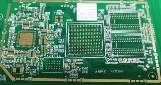
PCB Board Screen Printing refers to the application of a thin, patterned layer of ink—commonly called the “silkscreen”—onto the surface of a printed circuit board. This ink layer typically displays reference designators, polarity marks, component outlines, logos, and manufacturing data. Beyond its visual role, it serves practical functions that affect assembly precision, serviceability, and traceability.
The process originated from traditional textile screen printing, adapted in the 1950s to meet the needs of early circuit boards. Over the decades, it evolved from manual application to automated stencil and photo-imaging techniques. In the early stages, errors such as ink smearing and misalignment were common, often resulting in scrap boards or rework. Modern PCB Board Screen Printing, however, leverages computer-to-screen (CTS) technology, automated registration, and UV-curable epoxy-based inks, achieving alignment tolerances within ±50 μm.
This evolution mirrors broader manufacturing trends toward high precision and automation, allowing manufacturers like JM PCB, a leader in advanced circuit fabrication, to deliver consistent silkscreen quality even on dense and miniaturized boards.
Screen Mesh: Typically made from stainless steel or polyester, with mesh counts ranging from 200 to 400. The mesh determines ink deposition thickness and printing resolution.
Emulsion Layer: Coated on the screen to create a stencil pattern through UV exposure and development.
Squeegee: Used to press ink through the mesh onto the PCB surface, ensuring uniform transfer.
Ink: Specialized PCB inks are formulated for adhesion, chemical resistance, and thermal stability. Epoxy-based inks remain the industry standard due to their durability.
Curing: Inks are typically thermally or UV-cured to achieve hardness and solvent resistance.
The intricate balance among these elements dictates the quality and longevity of the silkscreen layer. Variations in viscosity, pressure, or curing temperature can lead to printing defects such as bleeding, incomplete coverage, or poor legibility.
Unlike standard graphic printing, PCB Board Screen Printing must comply with tight tolerances and chemical compatibility standards. For example:
The ink must not interfere with solderability or component placement.
The printed text must remain legible under harsh conditions (e.g., reflow soldering temperatures of 250°C).
The ink’s dielectric properties must ensure no electrical leakage or surface contamination.
Additionally, the process integrates with design software. CAD-to-CAM data ensures that printed component identifiers match the actual layout, reducing assembly errors.
Each mark, logo, or designator carries meaning. The reference codes on the silkscreen guide automated optical inspection (AOI) and human assemblers alike. Without precise PCB Board Screen Printing, errors in component placement can escalate during high-speed assembly lines.
Furthermore, regulatory and quality standards—such as IPC-6012 for rigid PCBs—require identifiable manufacturer information on each board. Thus, screen printing is not merely optional; it is a compliance requirement that ties into quality assurance and customer traceability systems.
PCB Board Screen Printing is typically performed after solder mask application and curing, but before final surface finishing or routing. The surface must be clean and smooth to ensure proper ink adhesion. Any contamination—residual flux, oil, or dust—can prevent ink bonding, leading to delamination during subsequent processes.
The quality of PCB Board Screen Printing depends heavily on the properties of the materials used. Ink chemistry, mesh material, and surface preparation all contribute to durability, clarity, and process repeatability.
Modern PCB inks are complex chemical formulations designed to balance adhesion, viscosity, and resistance. Common components include:
Epoxy Resin Base: Provides strong adhesion and mechanical durability.
Pigments: Give color contrast (usually white or yellow) against the green solder mask.
Solvents: Control the viscosity for smooth screen transfer.
Curing Agents: Promote cross-linking for hardness and resistance.
Additives: Improve flow, anti-foaming, and leveling properties.
The curing mechanism is vital. Thermal curing offers deeper cross-linking for better mechanical properties, whereas UV-curing inks allow for faster production and less thermal stress on substrates.
For optimal adhesion, the PCB surface energy must exceed that of the ink. Techniques such as plasma treatment or micro-abrasion are sometimes used to improve wetting characteristics before screen printing. Low surface energy areas (like PTFE-based laminates) may require special ink formulations.
As environmental regulations tighten, traditional solvent-based inks face restrictions. Manufacturers are moving toward low-VOC and halogen-free formulations. Moreover, high-reliability applications—such as aerospace and medical electronics—demand that the silkscreen layer withstand harsh environments without discoloration or degradation.
Although functionality is paramount, color and visibility remain important. White ink on a green solder mask is standard, but certain manufacturers use yellow, gray, or black inks for aesthetic or visibility reasons. The legibility of component codes affects not only assembly speed but also human error rates during inspection and rework.
| Defect Type | Possible Cause | Effect on Board Quality |
|---|---|---|
| Smearing or bleeding | Excessive ink or low mesh tension | Illegible text, aesthetic defects |
| Pinholes | Dust contamination | Incomplete markings |
| Misalignment | Poor registration or substrate shrinkage | Confusion during assembly |
| Poor adhesion | Inadequate curing or surface preparation | Ink peeling or flaking |
| Fading | UV degradation or low pigment density | Reduced readability |
Maintaining cleanroom-like conditions, precise ink viscosity control, and regular stencil maintenance are crucial preventive measures.
In the competitive landscape of PCB manufacturing, cost efficiency is a decisive factor that separates successful suppliers from lagging ones. While the silkscreen step may appear minor compared to processes such as copper plating or lamination, PCB Board Screen Printing contributes both direct and indirect costs that significantly affect the overall economics of production. A technical understanding of these cost elements helps manufacturers balance visual quality, throughput, and long-term reliability.
The direct costs of PCB Board Screen Printing include consumables, equipment depreciation, and labor. Although the ink consumption per panel is minimal, the cumulative effect across thousands of units can be substantial.
High-quality epoxy or UV-curable inks represent a small but critical expense. Ink prices vary based on formulation, brand, and performance characteristics—particularly thermal stability and adhesion. Low-cost inks might appear attractive initially, but they often result in fading, poor adhesion, or contamination issues that trigger costly rework.
A rough cost breakdown for a mid-volume production line might look like this:
| Cost Element | Approximate Contribution |
|---|---|
| Screen & Mesh Maintenance | 20% |
| Ink & Additives | 25% |
| Labor & Setup Time | 15% |
| Machine Depreciation | 25% |
| Quality Control & Rework | 15% |
This breakdown illustrates that even small variations in process efficiency or material quality can ripple through the production cost structure.
Modern automatic screen printers with computer-to-screen (CTS) alignment systems cost significantly more than manual setups. However, their precision and speed drastically reduce rework, thereby lowering the effective cost per unit over time. For large-scale PCB producers like JM PCB, this investment in automation ensures consistent results across multiple product lines.
Although largely automated today, the setup process—preparing the screen, registering the artwork, and calibrating squeegee pressure—still requires skilled technicians. A poorly aligned screen can render hundreds of panels defective, underlining the importance of trained operators.
Indirect costs often exceed direct expenses, especially when print quality affects downstream assembly or inspection processes.
Yield Impact: Poor legibility or misaligned markings can cause assembly errors or misidentification, lowering yield rates.
Rework Costs: Cleaning and reprinting silkscreens on assembled PCBs is labor-intensive and time-consuming.
Downtime: Clogged screens, improper curing, or equipment malfunctions may halt production lines, increasing overhead.
When multiplied across thousands of boards, even a 1% reduction in yield due to screen-printing defects can result in significant financial losses.
Continuous improvement through process optimization can drastically improve the cost-benefit ratio of PCB Board Screen Printing. Key strategies include:
Ink Viscosity Control: Maintaining a consistent viscosity prevents excessive ink use and reduces cleanup frequency.
Automated Vision Inspection: Real-time AOI after printing can detect misalignment or missing designators before curing.
Digital Screen Imaging (DSI): Eliminates film preparation and reduces setup time, increasing throughput.
Predictive Maintenance: Using machine learning algorithms to predict stencil wear and prevent downtime.
Each of these innovations contributes to operational efficiency and cost predictability—two pillars of modern manufacturing excellence.
Ultimately, the cost efficiency of PCB Board Screen Printing cannot be evaluated in isolation. The process affects not only aesthetics but also the mechanical and electrical performance of the board. Cheaper inks or shortcuts in curing may lower immediate costs but lead to failures during soldering, testing, or long-term usage.
In the intricate tapestry of PCB manufacturing, PCB Board Screen Printing stands as both a technical and symbolic process—marking the culmination of design, precision, and craftsmanship. Far from being a superficial aesthetic step, it contributes tangibly to product performance, reliability, and traceability.
The discipline of silkscreening unites material science, process engineering, and data integrity. Every printed character is a bridge between the physical and digital worlds, guiding assembly, supporting inspection, and ensuring long-term identification. As technologies like AI, automation, and sustainable chemistry mature, screen printing will remain integral to achieving consistent, high-quality PCB production.
Ultimately, beyond the visible markings lies a profound truth: PCB Board Screen Printing is not merely an afterthought—it is the final engineering signature that seals the identity and integrity of every circuit board.
Q1: What is PCB Board Screen Printing, and why is it necessary?
A1: PCB Board Screen Printing is the process of applying ink to the circuit board’s surface to create component labels, polarity marks, and manufacturer identifiers. It plays a critical role in ensuring that components are correctly placed during assembly and that technicians can trace and inspect the board easily. Without screen printing, assembly errors, maintenance difficulties, and traceability issues would increase dramatically.
Q2: What materials are used in PCB Board Screen Printing?
A2: The most commonly used materials are epoxy-based inks and UV-curable inks. Epoxy inks offer strong adhesion and chemical resistance, while UV inks cure quickly and provide excellent print precision. White is the most common color, but other colors like yellow or black can be used depending on the solder mask and visual contrast requirements.
Q3: How does PCB Board Screen Printing impact manufacturability?
A3: PCB Board Screen Printing affects manufacturability by influencing how easily assemblers can identify and place components. Clear markings reduce human errors, speed up production, and simplify automated optical inspection (AOI). Poor-quality printing can lead to confusion during assembly, resulting in rework or scrap.
Q4: What are the differences between traditional screen printing and digital printing in PCB manufacturing?
A4: Traditional screen printing uses a stencil and squeegee to apply ink, which is cost-effective for mass production but less flexible for small batches. Digital inkjet printing, on the other hand, uses precise nozzles to print directly onto the PCB surface. It offers higher resolution, faster setup, and easier design changes, making it ideal for prototyping and high-mix, low-volume production.
Q5: How does PCB Board Screen Printing contribute to traceability?
A5: Screen printing allows manufacturers to include identifiers such as serial numbers, batch codes, and barcodes directly on the board. These markings enable product tracking throughout the supply chain, simplify warranty management, and support quality control audits.


Connect to a Jerico Multilayer PCB engineer to support your project!
Request A Quote


 Quote
Quote