


+86 13603063656
Before diving into technical details, it is essential to clearly define what PCB Drilling encompasses and why it is central to the reliability of modern circuit boards.
PCB Drilling is the process of creating holes in printed circuit boards to enable interlayer electrical connections or to accommodate component leads. These holes may serve various purposes:
Through-holes: Pass completely through all layers, connecting the top to the bottom.
Blind vias: Connect outer layers to one or more inner layers.
Buried vias: Connect only internal layers, invisible from the surface.
The drilling process typically employs mechanical drills or laser drilling systems, depending on board complexity and hole size. Mechanical drilling remains dominant for through-holes and larger vias, while laser drilling is preferred for microvias in high-density interconnect (HDI) boards.
The quality of PCB Drilling depends on a variety of parameters—tool selection, spindle speed, feed rate, entry and exit materials, stack height, and environmental conditions. Each factor directly affects the hole wall smoothness, dimensional accuracy, and copper plating adhesion in subsequent processes.
A precise PCB Drilling operation ensures:
Minimal hole wall roughness for uniform copper deposition.
Consistent hole diameter within tolerance limits.
Accurate registration between hole and pad centers.
No burrs or resin smear that could compromise insulation resistance.
In other words, drilling quality determines the effectiveness of metallization and interconnection integrity, serving as the first checkpoint of PCB reliability.

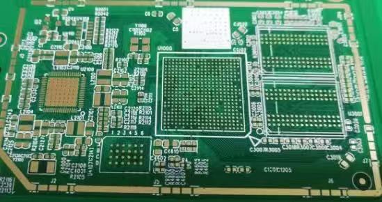
PCB Drilling
The link between PCB Drilling and circuit performance may not be visually apparent, but its effects are measurable and critical. Poorly drilled holes lead to uneven plating, inconsistent current flow, and potential hotspots in the circuit.
The electrical resistance of a plated through-hole depends heavily on the smoothness and cleanliness of the drilled wall. If PCB Drilling produces microcracks or resin residue, copper deposition during the plating process may not adhere uniformly. This results in increased contact resistance or intermittent electrical failure under thermal stress.
In high-speed and high-frequency applications, impedance stability is paramount. Misaligned vias caused by subpar PCB Drilling can disrupt trace geometry, creating impedance discontinuities that degrade signal quality. Even microscopic shifts can lead to reflection losses, especially in multilayer boards designed for RF or high-speed digital transmission.
Thermal management also depends on the quality of the drilled vias. When PCB Drilling achieves consistent hole walls and precise registration, thermal vias efficiently dissipate heat from hot components to inner or bottom layers. Conversely, poor drilling quality limits heat flow, accelerating material fatigue and reducing product lifespan.
In essence, PCB Drilling serves as both an electrical and thermal conduit. Its precision not only influences immediate circuit behavior but also determines long-term reliability under varying operating conditions.
In the competitive world of electronics manufacturing, cost efficiency must never come at the expense of quality. Achieving high-quality PCB Drilling while maintaining cost control requires a deep understanding of the factors that drive both.
Drill bits represent a major cost component in the PCB Drilling process. High-speed steel (HSS) or carbide drills are commonly used, with diameters as small as 0.1 mm in advanced HDI boards. Each bit has a limited lifespan, typically measured in the number of holes it can reliably produce. Worn bits generate excessive heat and rough hole walls, leading to defects that reduce plating adhesion and increase scrap rates.
Monitoring drill wear and implementing predictive tool replacement schedules are vital cost-control strategies that prevent quality degradation.
Drilling multiple panels at once increases throughput but introduces potential issues with registration accuracy and hole quality. Optimizing the PCB Drilling stack height—typically three to four panels per stack—balances productivity and precision. Excessive stacking increases tool deflection and burring, leading to costly rework or yield loss.
Energy consumption and bit life are directly linked to drilling parameters. Excessive spindle speed generates heat, causing resin smear, while low speed may increase cycle time. Intelligent process control systems now dynamically adjust parameters during PCB Drilling to maintain consistent results while reducing energy waste.
Automation plays a growing role in cost-efficient PCB Drilling. Advanced CNC systems equipped with real-time feedback and hole-count monitoring reduce operator error and scrap. Automation also ensures consistent bit alignment and minimizes downtime between tool changes.
Manufacturing yield—the ratio of functional boards to total boards produced—is one of the most crucial indicators of fabrication efficiency. The yield impact of PCB Drilling often extends beyond the drilling stage itself, influencing subsequent plating, lamination, and testing processes.
When PCB Drilling produces clean and consistent holes, the subsequent electroless copper deposition forms uniform conductive layers. In contrast, irregularities such as resin smear, delamination, or rough edges hinder copper adhesion, leading to poor plating coverage and early failures during reliability testing.
Multilayer PCBs depend on precise alignment between drilled holes and internal pads. Misalignment as small as 50 microns can cause open circuits or short connections after plating. Advanced PCB Drilling systems employ optical registration technology to align each panel layer with sub-micron precision.
Modern PCB Drilling machines feature sensors that monitor torque, vibration, and acoustic signatures during operation. By analyzing these signals, manufacturers can detect bit breakage or entry/exit burr formation in real time. This proactive approach reduces defective holes and improves overall yield.
The performance of PCB Drilling is not determined solely by the equipment or process parameters — the base materials themselves have an equally profound influence. The composition, density, and mechanical strength of PCB laminates directly affect hole wall quality, bit wear, and registration accuracy.
Modern PCBs are composed of composite materials like FR-4 (epoxy glass fiber), polyimide, Rogers laminates, or metal-core substrates. Each has distinct mechanical and thermal behaviors that influence the PCB Drilling process.
FR-4: The most common material, offering good drillability and moderate thermal resistance. However, it generates glass fiber dust that accelerates tool wear.
Polyimide: Used in flexible and high-temperature applications; it has lower mechanical rigidity, requiring slower drilling speeds to prevent tearing.
High-frequency laminates (e.g., PTFE-based): Soft and elastic, demanding precise feed rates to avoid burr formation and deformation.
Metal-core boards (MCPCB): Include aluminum or copper cores that require specialized drill bits and cooling systems to handle high thermal conductivity.
Each substrate dictates the spindle speed, feed rate, and chip load required for optimal drilling outcomes. Failure to adjust parameters according to material type can result in hole wall damage, delamination, or excessive tool wear.
Thicker copper foils and higher layer counts increase the challenge of PCB Drilling precision. The drill must penetrate multiple copper-clad layers without causing smear or burrs. In high-layer-count boards, even slight misalignment can propagate across layers, leading to connectivity defects.
Optimizing drill entry and backup materials, such as aluminum entry sheets and phenolic backers, helps achieve clean hole entry and exit while minimizing burr formation. These materials also dissipate heat and stabilize the drilling trajectory.
The glass transition temperature (Tg) of the PCB material affects how it behaves under drilling-induced heat. Low-Tg materials may soften, leading to resin smear along the hole walls. High-Tg materials resist thermal deformation but require higher spindle speeds and improved chip evacuation.
Selecting materials with appropriate Tg values for the intended drilling conditions ensures better hole integrity and long-term reliability.
Different materials introduce different defect mechanisms during PCB Drilling, summarized as follows:
| Material Type | Common Drilling Defect | Preventive Strategy |
|---|---|---|
| FR-4 | Resin smear, fiber pull-out | Use sharp carbide bits, optimize spindle speed |
| Polyimide | Delamination, tearing | Reduce feed rate, apply laser-assisted drilling |
| PTFE | Burrs, deformation | Use micrograin bits, maintain cooling air flow |
| MCPCB | Bit breakage, burrs | Employ diamond-coated drills, precise torque control |
Understanding material-specific behaviors allows manufacturers to optimize drilling recipes and reduce rework rates.
The journey of an electronic product — from conceptual circuit design to a fully functioning device — is paved with thousands of intricate details, each demanding precision. Among these, PCB Drilling stands as a quiet yet indispensable foundation. Its influence on yield, reliability, and performance is both fundamental and far-reaching.
Reliability in PCB manufacturing does not begin with assembly or testing — it begins deep within the substrate, where drilling defines the geometry and integrity of electrical pathways. A single deviation in hole size or misalignment can result in failures that no amount of downstream inspection can fully correct. Thus, PCB Drilling is not just a process; it is the precision blueprint for every electrical connection that follows.
Yield is the language of manufacturing success. When the drilling stage performs consistently, the entire production line benefits — plating quality improves, lamination defects decrease, and testing yields rise. The integration of smart drilling systems and adaptive process control transforms what was once an error-prone mechanical operation into a finely tuned digital ecosystem.
Manufacturers who invest in process data analytics, such as JM PCB, consistently demonstrate that cost and quality need not be at odds. By optimizing bit wear cycles, spindle speeds, and registration algorithms, they achieve both operational savings and superior yields — a balance that defines modern manufacturing excellence.
Material science plays a decisive role in drilling success. The choice of laminate, copper thickness, and dielectric structure determines how holes behave under mechanical stress. Understanding these relationships empowers engineers to design drilling strategies that minimize delamination, ensure stable impedance, and extend the lifespan of the finished board. The synergy between materials and PCB Drilling processes embodies the art of precision engineering.
Sustainability in PCB Drilling has evolved beyond energy efficiency; it now represents a commitment to responsible innovation. From recyclable materials and eco-friendly lubricants to intelligent dust management systems, each improvement contributes to a cleaner production environment. The industry’s push toward carbon-neutral manufacturing reaffirms that technological advancement can coexist with environmental stewardship.
Automation and artificial intelligence have transformed PCB Drilling into a data-driven science, yet human expertise remains irreplaceable. Skilled engineers interpret vibration data, detect subtle anomalies, and fine-tune parameters based on experience that machines cannot replicate. The best manufacturing facilities blend machine precision with human insight — a partnership that ensures every drilled hole meets not just technical specifications but also reliability expectations.
Looking ahead, PCB Drilling will continue evolving toward greater miniaturization, speed, and intelligence. As 5G, automotive radar, and AI hardware demand smaller vias and higher signal integrity, laser-drilling systems and hybrid mechanical-laser setups will dominate production. Advanced monitoring — combining acoustic sensing, real-time imaging, and predictive AI models — will make defects almost extinct.
Ultimately, the future of drilling is about integration: integrating data, design feedback, sustainability goals, and human ingenuity. In this convergence lies the foundation of next-generation electronics — reliable, efficient, and responsible.
In PCB fabrication, reliability is invisible until it fails. Every flawless product owes its success to precise, disciplined PCB Drilling. When engineers respect this process — controlling every parameter, inspecting every hole, and learning from every dataset — they do more than manufacture boards. They build trust into technology itself.
The core purpose of PCB Drilling is to create interlayer connections that enable electrical continuity between stacked copper layers. Without accurately drilled vias and through-holes, multilayer boards cannot function. These holes are later metallized with copper to form conductive pathways, connecting the inner circuitry that defines high-speed and high-density PCB performance.
Resin smear occurs when the heat generated during drilling melts the epoxy resin, causing it to smear along the hole walls. It can block copper connection points and hinder plating adhesion. To prevent this, manufacturers use sharp carbide bits, proper spindle speed, optimized feed rates, and entry materials that absorb heat and debris.
A worn drill bit produces uneven holes, rough walls, and higher localized heat, all of which can lead to plating failure and reduced insulation resistance. Predictive maintenance systems that track drill life and replace bits before failure are essential for ensuring consistent reliability.
Mechanical drilling uses physical bits to create holes, making it ideal for through-holes and larger vias. Laser drilling, however, vaporizes material with controlled energy bursts and is used for microvias or fine features in HDI boards. While mechanical drilling is faster for larger holes, laser systems provide unmatched precision for small and shallow features.
Cost control involves optimizing bit usage, minimizing rework, and using automation to reduce human error. Intelligent CNC systems adjust parameters automatically based on material feedback. Companies like JM PCB demonstrate how integrating data analytics into drilling can reduce energy costs and scrap rates while improving yield.


Connect to a Jerico Multilayer PCB engineer to support your project!
Request A Quote


 Quote
Quote