


+86 13603063656
In modern electronics, achieving high assembly yield and product reliability is no longer a matter of chance; it requires precise engineering at every stage of PCB production. Among the various factors affecting PCB performance, PCB Hole Tolerance plays a pivotal role. This seemingly minor detail in the design and fabrication process can influence soldering accuracy, component placement, mechanical stability, and ultimately, the long-term reliability of the product.
Manufacturers today face increasing pressure to produce smaller, faster, and more complex devices. The demand for high-density boards, fine-pitch components, and multilayer constructions amplifies the importance of maintaining strict PCB Hole Tolerance. Even a slight deviation from the intended hole diameter or position can result in misaligned components, soldering defects, and compromised electrical connections. These defects not only lower assembly yield but also threaten the operational life of the final product.
This article delves deep into the critical relationship between PCB Hole Tolerance, assembly yield, and product reliability. It highlights the methods used to control and measure tolerance, explains its impact on manufacturing and end-use performance, and provides practical guidance for designers and manufacturers. Throughout this discussion, real-world examples, best practices, and industry insights—including recommendations from trusted manufacturers like JM PCB—will illustrate the practical importance of managing PCB hole tolerances effectively.

PCB Hole Tolerance
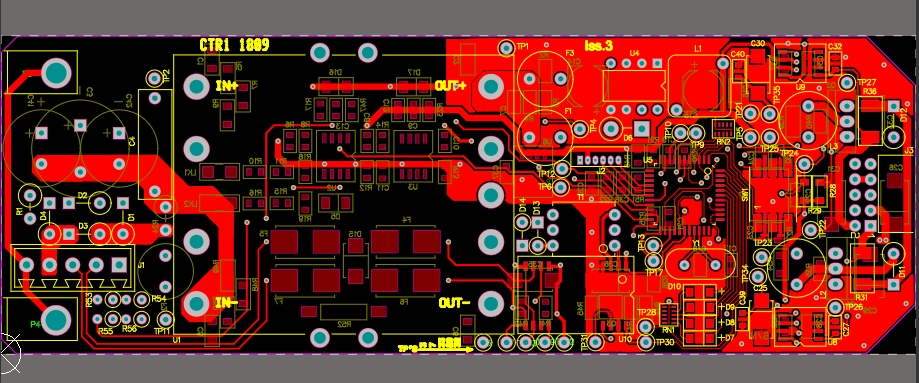
PCB Hole Tolerance refers to the permissible deviation from the nominal size and location of a drilled hole on a printed circuit board. These deviations are critical because even minimal misalignments can lead to improper component placement, electrical discontinuities, or mechanical stress during operation. Tolerances are typically defined in micrometers (µm) for high-density boards and vary depending on the board type, hole diameter, and the intended application.
Standards such as IPC-2221 and IPC-6012 provide guidelines for acceptable hole tolerances in different PCB classes. For instance, a high-performance or aerospace PCB may require a tighter tolerance compared to a consumer-grade board due to the extreme environmental conditions it may face. Understanding these standards is essential for both PCB designers and fabricators, as adherence ensures that the board meets functional and reliability requirements.
The materials used in PCB fabrication directly influence achievable PCB Hole Tolerance. Copper foils, for instance, must maintain consistent thickness and surface quality to support uniform plating and prevent deviation during drilling. Laminates, such as FR-4 or high-frequency materials, can expand or contract under thermal stress, affecting hole positioning. Plating techniques, whether electrolytic or chemical, must be controlled to maintain precise hole diameters without over- or under-plating, which can alter the intended tolerance.
Engineers often weigh the trade-offs between material cost and performance. For example, using high-quality, low-expansion laminates may slightly increase production costs but significantly improve hole tolerance, leading to fewer assembly defects.
Measuring PCB Hole Tolerance requires precision instruments and standardized methods. Common practices include:
Optical measurement systems: Cameras capture images of drilled holes, comparing them against nominal specifications.
Coordinate measuring machines (CMM): These provide highly accurate three-dimensional measurements of hole positions.
Drill hit analysis: Tracks the performance of drilling machines over time to ensure repeatability and detect deviations early.
These measurement techniques are vital not only for quality assurance but also for identifying potential issues before the PCB moves into assembly, thereby reducing rework and scrap rates.
High-density PCBs, commonly used in smartphones, servers, and aerospace applications, often have thousands of vias per square inch. In such boards, even a small deviation of a few microns in PCB Hole Tolerance can lead to significant misalignment during component placement. Companies that meticulously control tolerance during drilling and plating phases—like JM PCB—report a measurable reduction in assembly defects and improved product reliability. The careful integration of precision drilling, high-quality materials, and thorough inspection processes ensures that the hole tolerance is consistently within specification, ultimately supporting higher assembly yield and device longevity.
Accurate component placement is fundamental to achieving high assembly yield. PCB Hole Tolerance directly impacts this process because any deviation in hole diameter or position can misalign component leads or pads. For through-hole components, even a fraction of a millimeter difference can cause the part to sit unevenly on the board, resulting in poor solder joint formation and potential functional failure.
In surface-mount technology (SMT), vias and plated-through holes serve as thermal reliefs or electrical connections. Tolerance deviations can lead to uneven solder flow, affecting pad wetting and joint reliability. Designers must consider these tolerances during layout and specify hole sizes that accommodate the expected manufacturing variability. By maintaining tight PCB Hole Tolerance, assembly errors are minimized, and overall yield is improved.
Soldering, whether wave, reflow, or selective, depends heavily on the precise geometry of the PCB. Inconsistent hole sizes or misaligned vias due to poor PCB Hole Tolerance can cause:
Incomplete solder joints
Excessive solder bridging
Tombstoning of small components
Manufacturers often observe that a batch of boards with improperly controlled tolerances results in higher rework rates. By strictly managing PCB Hole Tolerance, solder paste deposition, heat transfer during reflow, and final joint quality can be optimized, leading to fewer defects and a more predictable assembly process.
Optimized PCB Hole Tolerance plays a preventive role in defect reduction. For example:
Drilling precision: Using laser drilling or high-quality mechanical drills ensures minimal deviation.
Plating control: Uniform copper plating inside vias prevents hole size reduction or irregularities.
Thermal management: Laminates with low expansion coefficients reduce dimensional changes during thermal cycles.
By integrating these strategies, manufacturers can reduce common assembly defects such as solder bridges, pad lifting, or misaligned leads. JM PCB, for instance, emphasizes strict hole tolerance monitoring during production, achieving higher first-pass yields and reduced scrap rates for clients in high-reliability markets.
PCB designers can take several proactive steps to ensure PCB Hole Tolerance does not compromise assembly yield:
Specify realistic tolerances: Align hole sizes with the capabilities of the manufacturer.
Avoid excessive via density: Overcrowding increases the risk of misalignment and soldering issues.
Include manufacturing allowances: Consider drill wander, plating thickness, and thermal expansion in design calculations.
Communicate with fabricators: Close collaboration with manufacturers like JM PCB ensures that tolerances are achievable and cost-effective.
Simulate assembly: Use CAD tools to model soldering behavior and predict tolerance-related problems before fabrication.
By considering these factors early in the design phase, engineers can prevent common assembly issues and ensure a higher-yielding production process.
The electrical reliability of a PCB is intrinsically linked to the precision of its holes. Deviations beyond the specified PCB Hole Tolerance can lead to intermittent connections, increased resistance, or even short circuits over time. In high-speed or high-frequency applications, even minor misalignments can introduce parasitic capacitance and signal integrity issues.
For example, in multilayer PCBs, vias often act as critical paths for signal transmission. If these vias are out of tolerance, the electrical path may be elongated or misaligned, causing delays or reflections. By maintaining tight PCB Hole Tolerance, engineers can ensure consistent electrical performance, reduce noise, and enhance overall signal integrity.
PCBs are subjected to mechanical stresses during assembly, transport, and operation. Misaligned or improperly sized holes increase localized stress, particularly around through-hole components. Over time, these stresses can lead to:
Via barrel cracking
Pad lifting
Delamination of the PCB layers
Maintaining proper PCB Hole Tolerance mitigates these mechanical failures. High-quality fabricators, such as JM PCB, employ precision drilling, controlled plating, and rigorous inspection to ensure that holes are within specification. This approach minimizes mechanical stress and significantly enhances product reliability, especially in high-vibration environments like automotive or aerospace electronics.
Electronic devices frequently experience temperature fluctuations that cause expansion and contraction of PCB materials. If PCB Hole Tolerance is not controlled, thermal cycling can exacerbate misalignments, leading to solder joint fatigue and eventual electrical failure.
Laminates with low thermal expansion coefficients, along with accurate hole drilling and plating, are essential for mitigating these effects. Proper tolerance ensures that vias and through-holes maintain their intended geometry despite repeated heating and cooling cycles, preserving both mechanical integrity and electrical connectivity.
JM PCB provides a practical example of how meticulous PCB Hole Tolerance management enhances product reliability. By integrating precision laser drilling, automated optical inspection, and strict plating control, JM PCB ensures that the dimensional accuracy of each hole meets the most demanding specifications.
Clients in sectors such as medical devices, aerospace, and telecommunications benefit from this approach. Reduced rework, minimized mechanical stress, and enhanced electrical consistency directly translate into higher long-term reliability of the final products. This demonstrates that PCB Hole Tolerance is not merely a design parameter—it is a strategic factor that safeguards the functionality and lifespan of electronic devices.
The choice of drilling method plays a crucial role in achieving precise PCB Hole Tolerance. Traditional mechanical drills are widely used for larger holes but may struggle to maintain tight tolerances in high-density boards. Drill wear, deflection, and vibration can result in slight deviations that accumulate across the board.
Laser drilling, on the other hand, offers significantly higher precision. It is ideal for microvias and high-density interconnects, where tolerances are measured in microns. Laser drilling ensures consistent hole size and location, reducing the likelihood of misalignment and assembly defects. For manufacturers seeking high reliability and minimal rework, combining mechanical drilling for larger holes with laser drilling for fine-pitch vias provides an effective hybrid solution.
Plating processes, particularly copper plating inside vias, can either enhance or compromise PCB Hole Tolerance. Uneven plating can reduce hole diameter, making component insertion difficult and affecting soldering quality. Conversely, over-plating may lead to irregular surfaces that cause poor contact and mechanical stress.
Controlled electrolytic and chemical copper plating techniques ensure uniform deposition, preserving the nominal hole diameter within tight tolerances. Advanced plating controls, often monitored by in-line inspection systems, are essential for boards used in high-reliability sectors. Maintaining consistent plating thickness also supports better thermal management, as uniform copper distribution improves heat conduction through vias.
Multilayer PCBs introduce additional complexity to PCB Hole Tolerance. Drilling must pass through multiple stacked layers with varying material properties, making precise alignment critical. Any misregistration between layers can result in incomplete or shorted connections.
To address this, manufacturers employ:
Stacked layer alignment techniques using optical registration
Sequential lamination processes to minimize layer shift
Advanced drilling equipment capable of maintaining consistent depth and location
These strategies ensure that holes maintain their intended diameter and alignment across all layers, which is particularly important for high-speed digital or RF applications where tolerances directly affect signal performance.
Rigorous inspection and quality control are indispensable for managing PCB Hole Tolerance. Common practices include:
Automated optical inspection (AOI): Detects misaligned or incorrectly sized holes before assembly
X-ray inspection: Evaluates the integrity of plated-through holes and detects voids
Statistical process control (SPC): Monitors drilling and plating processes to maintain consistency
By implementing comprehensive inspection protocols, manufacturers can ensure that every PCB meets design specifications. This approach not only improves assembly yield but also reduces the risk of reliability failures in the field.
High-quality fabricators, including JM PCB, emphasize these controls, providing customers with boards that consistently meet tight tolerances, reducing post-production defects and enhancing overall product quality.
PCB Hole Tolerance is a foundational element in modern electronics manufacturing, bridging the gap between design, fabrication, assembly, and product reliability. Its influence extends beyond mere dimensional accuracy, directly impacting assembly yield, soldering consistency, electrical performance, and long-term device stability.
Throughout this article, we have explored:
The fundamental principles of PCB Hole Tolerance—its definition, measurement methods, and material influences.
The impact on assembly yield—how precise tolerances reduce misaligned components, soldering defects, and rework rates.
The effect on product reliability—ensuring mechanical integrity, thermal stability, and consistent electrical performance.
Manufacturing techniques—from precision drilling and plating to multilayer alignment and rigorous inspection practices.
Design considerations—layout strategies, component footprint optimization, DFM integration, and simulation tools to predict tolerance effects.
Real-world applications and case studies—demonstrating how aerospace, high-speed digital, and consumer electronics benefit from tight hole tolerance, including insights from JM PCB.
Future trends—advances in drilling, plating, AI-driven optimization, miniaturization challenges, and smart inspection systems.
PCB Hole Tolerance is not merely a technical specification; it is a strategic enabler of performance, yield, and reliability. Companies that invest in understanding, controlling, and optimizing hole tolerances—through precise fabrication methods, advanced materials, and collaborative design practices—gain measurable advantages in both quality and cost-efficiency.
In conclusion, mastering PCB Hole Tolerance is essential for bridging the critical link between design intent and real-world performance. By integrating precise tolerance control into every stage of the PCB lifecycle—from material selection and drilling to plating, assembly, and inspection—engineers can confidently achieve higher assembly yields, robust product reliability, and long-term customer satisfaction.
Rolled copper foil is produced by mechanically rolling copper into thin sheets. This method provides superior surface quality, mechanical strength, and uniform thickness, making it ideal for high-frequency or high-reliability PCBs. Electrolytic copper foil, in contrast, is deposited via an electrolytic process. It is more flexible and cost-effective, but may exhibit less uniformity in thickness and mechanical strength.
Both types of foil impact PCB Hole Tolerance, as variations in copper thickness can influence the final hole diameter after plating and drilling. Engineers must select the appropriate foil type based on tolerance requirements, electrical performance, and cost considerations.
For high-density PCBs, PCB Hole Tolerance typically ranges from ±5 µm to ±25 µm depending on via size, board thickness, and application. Tighter tolerances are critical for fine-pitch components and multilayer boards, where misalignment can result in soldering defects, poor electrical performance, and reduced reliability. Designers must coordinate with manufacturers to ensure achievable tolerances that balance cost and yield.
Yes. PCB Hole Tolerance affects the consistency and conductivity of plated-through vias, which often serve as thermal conduits between layers. Deviations in hole size or plating thickness can reduce heat transfer efficiency, potentially causing localized hotspots. Accurate control of hole tolerance ensures effective thermal management, especially in power electronics and high-performance computing applications.
Several inspection techniques are used to verify PCB Hole Tolerance, including:
Automated optical inspection (AOI): Detects misaligned or incorrectly sized holes.
X-ray inspection: Evaluates via integrity and detects voids.
Coordinate measuring machines (CMM): Provide precise 3D measurements of hole location and diameter.
Drill hit analysis: Monitors drill consistency over time.
These methods help maintain yield and reliability by identifying tolerance deviations early in the production process.
Yes. JM PCB specializes in providing customized PCB Hole Tolerance solutions tailored to client requirements. By combining precision drilling, controlled plating, and comprehensive inspection, JM PCB ensures tight tolerance control for high-density, high-reliability, and critical application PCBs. Their approach helps clients reduce assembly defects, improve first-pass yield, and enhance long-term product reliability.


Connect to a Jerico Multilayer PCB engineer to support your project!
Request A Quote


 Quote
Quote