


+86 13603063656
In the high-speed, high-density world of modern electronics, the importance of signal integrity cannot be overstated. As circuit layouts become denser and transmission speeds increase, even minor inconsistencies in the printed circuit board (PCB) structure can translate into signal loss, crosstalk, or timing errors. At the center of this challenge lies a crucial but sometimes overlooked factor—PCB Insulation. The quality, type, and design of PCB Insulation not only protect the copper traces and vias but also play a decisive role in how signals propagate across layers.
This article explores in depth how advanced PCB Insulation technologies contribute to signal integrity, thermal stability, and long-term reliability. We will examine what PCB Insulation is, its various forms, how it affects PCB performance, and the available solutions for common insulation challenges.
PCB Insulation
At its core, PCB Insulation refers to the dielectric layers that separate conductive copper paths on a circuit board. These insulating materials prevent unwanted current flow, reduce interference, and provide mechanical stability. Without effective insulation, no PCB could reliably support today’s electronic devices.
Modern PCBs often include multiple insulation layers made from different materials such as FR-4 epoxy resin, polyimide, PTFE (Teflon), or other high-performance laminates. Each material has unique electrical properties (dielectric constant, dissipation factor), mechanical properties (glass transition temperature, moisture absorption), and cost profiles. Engineers must balance these factors to meet the requirements of high-frequency signals, power management, and environmental conditions.
By selecting appropriate PCB Insulation, designers can control impedance, minimize crosstalk, and achieve consistent high-speed performance. This is especially critical in industries like telecommunications, aerospace, automotive, and data centers, where the reliability of every bit transmitted matters.
One of the most important functions of PCB Insulation is controlling the electrical parameters of the board. Two key aspects stand out:
Dielectric Constant (Dk): This determines how quickly an electrical signal can propagate through the medium. Lower Dk materials support higher signal speeds and less signal distortion.
Dissipation Factor (Df): This indicates energy loss within the insulating material. Low Df materials minimize signal attenuation over distance.
As operating frequencies rise above several gigahertz, traditional FR-4 materials may no longer suffice. Advanced PTFE composites or ceramic-filled laminates offer improved Dk and Df values, making them ideal for high-speed PCBs. Choosing the right PCB Insulation helps engineers achieve controlled impedance and reduce the risk of reflections or losses.
Electrical performance is only part of the story; PCB Insulation also impacts heat dissipation. Poor insulation can trap heat and lead to delamination or premature failure of solder joints. High-temperature materials such as polyimide or high-Tg FR-4 can withstand soldering and reflow cycles without degrading.
The thermal conductivity of insulating layers affects how heat moves away from components. While copper planes primarily conduct heat laterally, dielectric materials influence the vertical path. Advanced formulations with ceramic fillers can improve thermal conductivity, enabling boards to handle higher power densities.
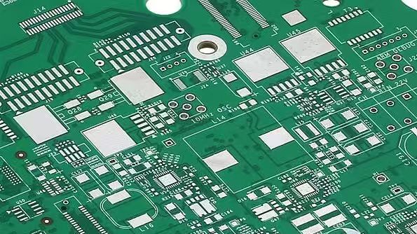
Beyond electrical and thermal factors, PCB Insulation must provide mechanical integrity. It needs to resist cracking, moisture ingress, and dimensional instability. As PCBs become thinner and more complex (e.g., HDI boards), the stresses during manufacturing and operation increase. Flexible PCBs, rigid-flex PCBs, and multilayer HDI designs all push the limits of insulation performance.
Choosing robust PCB Insulation materials and carefully controlling lamination processes ensure that the dielectric layers maintain their properties over the board’s lifetime.
Emerging insulation technologies focus on:
Low-loss materials for high-frequency and high-speed applications
Ultra-thin dielectrics to support finer trace geometries and increased layer counts
Environmentally friendly materials with lower halogen content and improved recyclability
Enhanced adhesion systems that minimize delamination under thermal stress
For example, next-generation PCB Insulation laminates from leading manufacturers combine resin systems with ceramic or PTFE micro-fillers to achieve both low dielectric loss and higher thermal conductivity. These innovations support applications like 5G infrastructure, satellite systems, and advanced automotive electronics.
Despite the advances, challenges remain in ensuring consistent PCB Insulation performance:
Moisture Absorption: Even small amounts of moisture can increase dielectric loss and cause delamination. Using low-absorption materials and controlled manufacturing environments helps mitigate this risk.
Thermal Expansion Mismatch: Copper and dielectric materials expand at different rates. Selecting materials with matched coefficients of thermal expansion (CTE) reduces stress during thermal cycling.
Void Formation: Incomplete resin filling or trapped air pockets weaken insulation. Vacuum lamination and proper prepreg selection minimize voids.
Aging and Chemical Exposure: Long-term exposure to harsh chemicals or UV can degrade insulation. Protective coatings and careful material selection help extend life.
By implementing these solutions, manufacturers can ensure that PCB Insulation layers remain stable and reliable even under extreme conditions.
While signal integrity often takes the spotlight, power integrity is equally critical in modern PCB design. Power delivery networks (PDNs) must provide clean, stable voltage to components. The performance of the dielectric layers directly influences how power is distributed across the board.
Low-impedance power planes separated by thin PCB Insulation layers can act as distributed capacitors, reducing voltage ripple. Conversely, poor dielectric choices with high dissipation factors can lead to noise propagation and increased power losses. High-performance insulation materials with stable dielectric properties over temperature and frequency enable better decoupling and lower impedance.
Furthermore, the dielectric’s thickness and uniformity help define the plane capacitance and, therefore, the overall transient response of the PDN. Designers who collaborate closely with PCB fabricators can specify insulation thicknesses within tighter tolerances, thus achieving more predictable power delivery.
The role of PCB Insulation in electromagnetic compatibility is often underestimated. EMC compliance depends on controlling emissions and susceptibility at the board level. Dielectric materials with consistent properties help maintain impedance control, reduce radiation, and improve shielding effectiveness.
Thin, uniform insulation layers between power and ground planes create return paths that minimize loop areas. This reduces the potential for electromagnetic radiation. Additionally, specialized materials with low permeability or embedded shielding structures can further improve EMC performance.
With high-frequency signals running at tens of gigahertz, every microstrip, stripline, and via transition matters. Advanced PCB Insulation materials ensure predictable impedance and reduce the risk of resonance effects that amplify noise.
High-density interconnect (HDI) boards push the limits of PCB Insulation technologies. Ultra-thin dielectrics, laser-drilled microvias, and sequential lamination all demand exceptional material performance and process control.
The insulation layers in HDI boards must:
Withstand multiple lamination cycles without degrading
Support very thin dielectric thicknesses (often less than 50 μm)
Maintain adhesion between copper and dielectric interfaces
Exhibit low outgassing to avoid voids in microvias
Materials like advanced epoxy resins, modified polyimides, or resin-coated copper (RCC) prepregs are commonly used. These enable extremely fine pitch components, higher layer counts, and improved signal routing density—all without sacrificing reliability.
Industrial, automotive, and aerospace applications often expose PCBs to temperature extremes, vibration, moisture, and aggressive chemicals. PCB Insulation materials for these applications must exceed standard requirements.
Key considerations include:
Temperature Resistance: High glass transition temperatures (Tg) and low coefficients of thermal expansion (CTE) prevent cracking and delamination during thermal cycling.
Moisture Resistance: Hydrophobic materials or protective coatings reduce moisture uptake and maintain dielectric performance.
Chemical Resistance: Certain industries require boards to withstand oils, fuels, or solvents without degrading insulation properties.
Long-term reliability studies show that premium PCB Insulation materials can extend product lifetimes by years compared to commodity-grade laminates.
As electronic systems evolve toward higher data rates and smaller footprints, PCB Insulation materials will continue to improve. Several trends are emerging:
Lower-Loss Resins: Materials with ultra-low Df to support 112 Gbps PAM4 and beyond
Nanofillers: Incorporating nano-scale particles to improve thermal conductivity and mechanical properties without increasing Dk
Flexible High-Speed Laminates: For foldable and wearable devices, combining flexibility with low-loss performance
Environmentally Sustainable Materials: Meeting RoHS, REACH, and halogen-free requirements while maintaining performance
Designers who keep pace with these trends can ensure that their boards remain competitive and future-proof.
Flexible and rigid-flex PCBs introduce unique challenges for PCB Insulation. Unlike standard rigid boards, these designs must withstand repeated bending, folding, and vibration without cracking or delaminating.
Key considerations for insulation in flexible and rigid-flex boards include:
Material Flexibility: Polyimide films are widely used for flexible PCBs because of their excellent bending endurance and high temperature stability.
Adhesive Systems: Flexible laminates often use adhesive or adhesiveless constructions. Adhesiveless laminates reduce thickness and improve bend performance, but require tighter process control.
Copper Foil Bonding: Rolled-annealed copper foil, due to its smooth grain structure, bonds more securely to flexible insulation materials and resists cracking during bending.
For rigid-flex designs, the transition areas between rigid and flexible sections must be carefully engineered. The insulation thickness, copper coverage, and neutral bending axis placement all influence long-term reliability. Advanced PCB Insulation materials and fabrication techniques make it possible to integrate high-density interconnects with flexible segments for dynamic applications such as medical catheters, foldable displays, and aerospace harnesses.
Because insulation layers form the backbone of electrical isolation, they must undergo rigorous testing to ensure compliance with industry standards. Typical PCB Insulation tests include:
Dielectric Breakdown Voltage (DBV): Measures the voltage at which the insulation fails.
Insulation Resistance (IR): Assesses how effectively the dielectric prevents leakage currents.
Moisture and Thermal Aging: Boards are subjected to high humidity and temperature cycles to evaluate long-term performance.
Cross-Sectional Analysis: Microscopy reveals voids, delamination, or improper resin fill between layers.
Time-Domain Reflectometry (TDR): Confirms controlled impedance and dielectric consistency at high frequencies.
These tests allow manufacturers to identify weaknesses before boards are assembled into critical systems. By partnering with suppliers who implement strict quality protocols, designers can be confident their PCB Insulation layers meet or exceed specifications.
While high-performance insulation materials bring clear benefits, they also influence the overall cost of a PCB. Factors include:
Raw Material Price: Advanced PTFE or ceramic-filled laminates can be several times more expensive than standard FR-4.
Manufacturing Complexity: Ultra-thin dielectrics and multiple lamination cycles add to fabrication costs.
Yield Impact: Tighter tolerances require more stringent quality control, which may reduce yield if not managed properly.
However, these costs are often justified when weighed against the savings from reduced signal integrity issues, lower power losses, and longer product life. A strategic approach is to segment designs by performance criticality—using premium PCB Insulation only where necessary while retaining standard materials elsewhere.
Several innovative directions are already reshaping the PCB Insulation landscape:
Embedded Capacitance Layers: Ultra-thin dielectrics act as distributed capacitors to improve power integrity.
Hybrid Material Stacks: Combining multiple dielectric types in one stackup to optimize cost, thermal performance, and electrical properties.
3D Printed Dielectrics: Additive manufacturing of insulation layers for custom geometries and rapid prototyping.
Advanced Surface Treatments: Plasma or laser texturing of copper and dielectric surfaces to enhance adhesion without extra thickness.
These developments suggest a future where insulation materials are tuned not only for electrical and thermal properties but also for manufacturability and sustainability.
The evolution of modern electronics has pushed PCBs into realms where tiny variations in materials and geometry can make or break a product. At the heart of this reliability lies PCB Insulation—a critical yet often overlooked component that governs electrical, thermal, and mechanical performance.
Throughout this article, we explored how PCB Insulation influences signal integrity, power delivery, electromagnetic compatibility, and long-term reliability. We examined the unique requirements for high-speed, high-density, flexible, and harsh-environment boards. We also highlighted solutions and testing methods to ensure insulation layers meet stringent standards.
Ultimately, investing in advanced PCB Insulation technologies is not just about meeting today’s performance goals; it’s about future-proofing designs for the next generation of speed, density, and environmental demands.
Answer: Rolled copper foil is produced by mechanically rolling copper into thin sheets, resulting in smoother surfaces and higher mechanical strength. Electrolytic copper foil is deposited via an electrolytic process, offering more flexibility and cost-effectiveness. Both types can be used in PCBs, but rolled copper foil is often chosen for applications requiring excellent flex performance and fine line definition, while electrolytic copper foil is popular for mass production due to its lower cost.
Answer: The thickness of the insulation layer between copper conductors defines the distance between signal traces and reference planes. Thinner insulation results in stronger capacitive coupling and lower impedance, while thicker insulation yields higher impedance. Accurate impedance control requires consistent dielectric thickness and material properties across the PCB.
Answer: For high-speed designs, low-loss materials such as PTFE (Teflon), ceramic-filled hydrocarbon resins, and advanced modified epoxy systems are common. These materials offer lower dielectric constants and dissipation factors compared to standard FR-4, which helps maintain signal integrity at high frequencies.
Answer: Moisture increases the dielectric constant and dissipation factor of insulating materials, leading to signal loss and possible impedance shifts. It can also cause delamination or corrosion at copper interfaces. Using low-moisture-absorption materials and protective coatings helps preserve insulation performance in humid or wet environments.
Answer: Crosstalk occurs when signals on one trace couple into neighboring traces. The dielectric constant and spacing defined by PCB Insulation directly affect the degree of coupling. Lower-Dk materials and thicker insulation reduce capacitance between traces, thereby minimizing crosstalk. Additionally, maintaining solid reference planes and controlled impedance throughout the stackup further suppresses interference.


Connect to a Jerico Multilayer PCB engineer to support your project!
Request A Quote


 Quote
Quote