


+86 13603063656
Printed Circuit Boards (PCBs) have evolved into highly sophisticated platforms capable of carrying power, signals, and mechanical support for virtually every modern electronic product. As designs become denser and more complex, PCB Slots—elongated cutouts or channels machined into the PCB—play a critical role in meeting mechanical, electrical, and thermal requirements. Understanding PCB Slots is essential for engineers and designers who want to improve manufacturability, reduce costs, and ensure long-term reliability.
This guide acts as a single resource covering all aspects of PCB Slots, from definition and types to manufacturing, cost considerations, and real-world best practices. It also integrates frequently asked questions and first-hand insights drawn from years of industry observation, giving designers and fabricators a real advantage.

PCB Slots
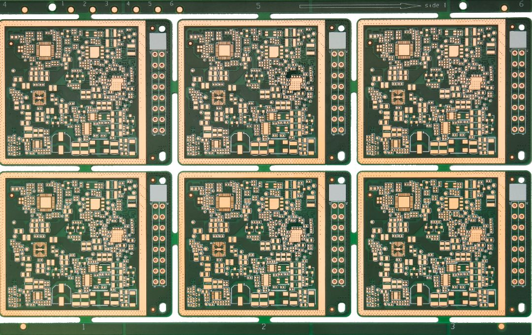
PCB Slots are non-circular openings cut into the PCB substrate. Unlike standard drilled holes or vias, PCB Slots are elongated and may have rounded or squared ends. Their width is typically determined by the router bit or laser beam used in the fabrication process. These slots can be plated or non-plated, depending on whether they need to carry electrical signals or simply provide clearance.
Key aspects include:
Mechanical accommodation: PCB Slots make room for connectors, components, or mechanical fixtures.
Thermal management: By providing airflow or physical separation, slots can help dissipate heat or isolate hot components.
High-voltage isolation: Slots can be used to increase creepage distances, improving insulation performance.
Weight reduction: In large PCBs, removing material with slots can reduce overall weight, important in aerospace and medical applications.
By incorporating PCB Slots thoughtfully, designers ensure the PCB supports both electrical and mechanical needs without increasing the board outline or complexity unnecessarily.
A major benefit of PCB Slots is their ability to save time in assembly and maintenance, as well as improve overall design efficiency. Here’s how:
Component Alignment
Slots allow connectors or edge components to align automatically during assembly, reducing manual adjustments.
By guiding components into place, PCB Slots reduce rework and lower the chance of misalignment.
Faster Prototyping
Using standardized PCB Slots dimensions enables faster prototyping since manufacturing houses already have toolsets for common slot widths.
This speeds up the turnaround time from concept to physical boards.
Reduced Assembly Steps
Some PCB Slots are designed to allow snap-fit components or board-to-board connectors, reducing the need for additional fasteners or soldering steps.
Enhanced Serviceability
PCB Slots allow easier removal of certain subassemblies or modules, saving time during maintenance or upgrades.
By saving time across the product’s lifecycle—from initial assembly to field servicing—PCB Slots contribute to both lower cost and improved reliability.
One of the challenges in designing PCB Slots is ensuring the board retains enough mechanical strength. Overuse or poor placement can lead to flexing or cracking during assembly.
Practical tips:
Place PCB Slots away from high-stress areas such as mounting points or connector edges unless they’re part of the mechanical interface.
Use filleted (rounded) ends rather than sharp corners to reduce stress concentration.
Consider thicker copper or additional stiffeners if large slots are necessary.
Balancing slot function with structural needs is an area where designers can differentiate themselves.
PCB Slots can be strategically placed to isolate high-voltage sections or improve creepage distance between conductive paths. In power electronics, for example, adding a slot between primary and secondary circuits of a transformer helps meet regulatory isolation requirements.
Additionally, in high-density designs, PCB Slots can create physical “moats” that break up ground planes or thermal paths. This approach can prevent localized heating or crosstalk between sensitive analog circuits and high-current digital traces.
In today’s high-speed designs, minimizing unwanted capacitance and crosstalk is critical. PCB-Slots can help shape return paths, reduce electromagnetic interference (EMI), and physically separate incompatible subsystems. When done correctly, this can:
Improve signal integrity
Reduce system noise
Enhance electromagnetic compatibility (EMC) performance
Slots can add cost to a PCB because they involve extra routing or laser cutting. To control expenses:
Combine multiple slots into a single cut path where feasible.
Use standard slot widths and shapes.
Discuss production panelization with your manufacturer to minimize scrap.
However, the time saved in assembly or improved reliability may offset the higher manufacturing cost of PCB-Slots.
While the fundamentals of PCB-Slots are relatively straightforward, their manufacturing has become increasingly sophisticated. Fabricators now deploy a variety of techniques depending on the slot’s function, tolerances, and the board’s material.
The most common method of creating PCB-Slots is mechanical routing. A high-speed spindle uses carbide bits or diamond-coated routers to cut the slot into the substrate. Mechanical routing is cost-effective for moderate tolerances and suitable for both plated and non-plated slots.
For very fine or complex slot shapes, laser machining is becoming popular. Ultraviolet (UV) and CO₂ lasers can cut small, precise slots with minimal mechanical stress. This process is especially valuable for rigid-flex or very thin PCBs.
Plated PCB-Slots carry electrical current or serve as part of a connector interface. Non-plated slots simply provide clearance or isolation.
Because slots are elongated, they’re more susceptible to cumulative error than simple holes. Ask your fabricator for their standard tolerances and use their recommendations.
As product volumes increase, the value of PCB-Slots as time-saving features multiplies. Here’s how they work in mass production:
Automated assembly line integration
Reduced fixture complexity
Faster quality assurance
Improved heat dissipation during reflow
By integrating PCB Slots thoughtfully, you can drastically reduce labor costs and time-to-market, especially in high-volume scenarios.
In rigid-flex designs, PCB-Slots allow the flex section to bend without interfering with stiffeners or components and can help control stress distribution at the rigid-flex junction.
For advanced substrates such as ceramics or high-frequency laminates, slot cutting requires special tooling and process control. Always consult your fabricator early when designing slots into exotic materials.
Beyond mechanical alignment and isolation, PCB-Slots can act as intentional electromagnetic and thermal features:
EMI control
Thermal relief
Creepage and clearance
These advanced uses demonstrate how PCB Slots can be an integral part of system-level engineering rather than just mechanical cutouts.
Modern PCB design isn’t complete without simulation, and PCB-Slots deserve equal attention.
Electrical simulation predicts impedance and EMI effects.
Thermal simulation shows how slots relieve hotspots.
Mechanical stress testing validates structural integrity under vibration or flexing.
Prototyping is the ideal stage to experiment with PCB Slots. Include a range of slot sizes or shapes on a single prototype, test thoroughly, and keep records for future projects.
Adding PCB Slots increases fabrication complexity but also yields measurable benefits. Conduct ROI analyses to weigh additional fabrication costs against assembly savings, improved reliability, and easier testing.
DFM reviews should always include a PCB Slots section. Working closely with your manufacturer early prevents costly re-spins and accelerates time-to-market.
In many industries—medical, automotive, aerospace—PCB Slots are part of compliance strategies for creepage distances, thermal safety, and isolation barriers.
The evolution of PCB Slots mirrors the evolution of PCBs themselves. As boards become denser, more integrated, and subject to harsher environments, the humble slot gains importance.
Future trends likely include:
Micro-slots in HDI designs
Integration with additive manufacturing
Smarter thermal designs using CFD-guided slot placement
With careful planning, simulation, and partnership with experienced fabricators like JM PCB, you can leverage PCB Slots to save time, enhance reliability, and meet aggressive cost and performance targets.
Q1: What is the difference between rolled copper foil and electrolytic copper foil?
Rolled copper foil is produced by mechanically rolling copper into thin sheets. It offers better surface quality and mechanical strength. Electrolytic copper foil is deposited via an electrolytic process and is more flexible and cost-effective.
Q2: How do PCB-Slots affect impedance and signal integrity?
Slots can influence the return path of high-speed signals, potentially increasing impedance or creating discontinuities.
Q3: What materials are most compatible with PCB-Slots?
FR-4 is most common. Polyimide-based rigid-flex boards handle stress better. High-frequency laminates and ceramics require special tooling.
Q4: How do I specify plated versus non-plated PCB-Slots in my design files?
Most fabricators prefer clear layer designations in Gerber or IPC-2581 files and a clear fabrication drawing.
Q5: Are there industry standards governing PCB-Slots?
IPC-2221 and IPC-6012 provide general guidance on mechanical features including slots. UL standards may also impose requirements on creepage distances


Connect to a Jerico Multilayer PCB engineer to support your project!
Request A Quote


 Quote
Quote