


+86 13603063656
Modern electronics are becoming denser, faster, and more power-hungry. This evolution creates a fundamental challenge: how to manage the heat generated within densely packed printed circuit boards (PCBs). While traditional approaches often focused on heat sinks, fans, or chassis cooling, these external solutions alone are no longer sufficient. The heat must be addressed at its source — inside the PCB itself.
PCB Thermal Management Technology is the discipline of designing boards, materials, and manufacturing techniques so that heat can be efficiently conducted away from critical components, ensuring the reliability and longevity of the entire system. This article will explore how the technology evolved, its benefits, best practices, and practical insights — including a few personal thoughts about the future of the field.

PCB Thermal Management Technology
PCB Thermal Management Technology involves the systematic integration of thermal considerations into PCB design, material selection, and manufacturing processes. At its core, it combines principles of thermal conductivity, fluid dynamics, and materials science.
Key aspects include:
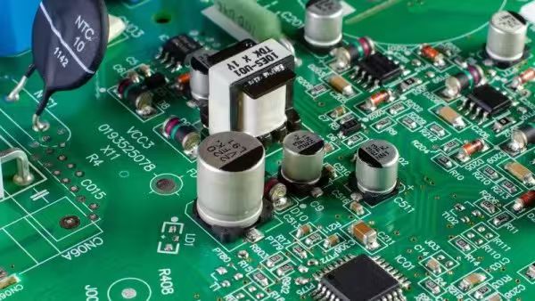
Thermal vias and heat-spreading planes that conduct heat away from hot components.
High thermal conductivity laminates such as metal-core PCBs or ceramic substrates.
Phase-change and interface materials to reduce thermal resistance between layers.
Advanced copper foils and high-fill via structures that improve conduction pathways.
From my perspective, the future lies in predictive simulation models — enabling engineers to virtually test thermal profiles before manufacturing a single prototype. This digital twin approach will further push PCB Thermal Management Technology from being a reactive afterthought to a proactive design pillar.
Reliability in electronics correlates strongly with operating temperature. For every 10 °C rise in temperature, component life may halve due to accelerated chemical and physical degradation. PCB Thermal Management Technology mitigates this risk by:
Keeping solder joints below fatigue thresholds.
Preventing delamination of multilayer boards.
Reducing electromigration risks in fine copper traces.
In my experience, the biggest gain comes from balancing thermal conductivity with manufacturability. Over-engineering the heat spreader might reduce flexibility during assembly or rework. Engineers must therefore find a sweet spot where performance and practicality intersect.
The main advantages include:
Improved Component Lifespan – By managing heat at the PCB level, semiconductors and passive components last longer.
Enhanced Signal Integrity – Lower thermal gradients reduce stress on high-speed interconnects.
Reduced Mechanical Stress – Boards maintain their dimensional stability, which preserves alignment for connectors and BGA packages.
Higher Power Density – Allows designers to pack more functionality into the same board footprint without risking overheating.
One practical recommendation is to partner with manufacturers experienced in high-performance materials. For example, JM PCB offers a wide range of boards with excellent thermal properties, which can significantly reduce the iteration cycle for high-power designs.
Material selection defines how well heat travels through the PCB stack-up. Common choices include:
FR-4 with enhanced thermal conductivity – Still cost-effective but better than standard FR-4.
Metal Core PCBs (MCPCBs) – Typically aluminum or copper cores that draw heat away.
Ceramic Substrates – High-end choice for extreme conditions, such as automotive power modules.
High-performance copper foils – Rolled copper foil vs. electrolytic copper foil; each has distinct properties.
Some design tactics:
Thermal Vias: Placed under hot components to transfer heat to internal copper planes.
Copper Pour and Plane Layers: Increase cross-section for heat flow.
Embedded Heat Pipes or Graphite Sheets: Advanced methods for high-density boards.
Component Placement Optimization: Hot parts should be spaced or arranged for airflow.
From my viewpoint, using computational fluid dynamics (CFD) early in layout dramatically improves outcomes. Designers can simulate airflow, convection, and conduction simultaneously.
Manufacturing is not just about making the board — it’s about maintaining thermal pathways. Factors include:
Ensuring via fill materials have consistent thermal properties.
Lamination cycles optimized to avoid micro-voids.
Surface finish selection (ENIG, HASL, OSP) with thermal behavior in mind.
Balancing copper thickness and etch tolerances.
Working with established vendors like JM PCB can streamline these challenges. They offer well-characterized processes for heavy copper and thermal via filling.
Testing ensures that the intended thermal performance actually exists. Techniques include:
Thermal Imaging under operational loads.
Thermocouples Embedded in Critical Zones during prototype testing.
Accelerated Life Tests with power cycling to stress thermal joints.
These practices are essential because real-world conditions often differ from lab assumptions. Personally, I think more collaboration between PCB designers and reliability engineers could lead to standardized “thermal readiness” ratings similar to IP or UL ratings today.
Material innovation is at the heart of PCB Thermal Management Technology. Over the past decade, the industry has moved beyond simply increasing copper weight or using thicker prepregs. Instead, engineers now explore composite resins, nano-filled dielectrics, and embedded metal layers. Each innovation is aimed at reducing the thermal resistance path between the component junction and the environment.
Nano-Filler Epoxies: These materials increase thermal conductivity of the dielectric without compromising dielectric strength.
Hybrid Ceramic-Polymer Laminates: Achieve high insulation resistance with superior heat conduction.
Graphene and Carbon-Based Inserts: Provide directional heat spreading capabilities.
From my perspective, the real breakthrough will come when we standardize these exotic materials for volume production — at which point PCB Thermal Management Technology will shift from being a premium feature to a mainstream necessity.
Before a PCB goes into production, its thermal profile can be digitally modeled. This is one of the fastest growing aspects of PCB Thermal Management Technology because it allows engineers to experiment with layer counts, copper thicknesses, and via densities virtually.
Predict Hotspots early.
Optimize Layer Stack-ups before fabrication.
Perform Cost-Benefit Analyses by weighing extra copper or vias against thermal performance gains.
ANSYS Icepak
Cadence Sigrity PowerDC
SolidWorks Flow Simulation
I recommend designers not just model steady-state conditions but also simulate transient spikes. This reflects the real-world behavior of power regulators, RF amplifiers, and automotive ECUs.
As packages like BGA, QFN, and chiplets shrink while power densities rise, the junction-to-board thermal path becomes more critical. PCB Thermal Management Technology addresses this by matching land patterns, pad geometries, and via configurations to the component’s thermal pad.
Direct Die-Attach to Copper Planes for high-power LEDs.
Embedded Heat Spreaders underneath CPU or ASIC zones.
Multiple Thermal Via Arrays under power MOSFETs.
In my view, the most underutilized tactic is co-design between PCB and package teams. When both are designed concurrently, the thermal path can be optimized holistically.
Applications such as automotive inverters, 5G base stations, and industrial drives push PCBs beyond their traditional limits. Here PCB Thermal Management Technology plays a critical role not only in cooling but also in maintaining signal integrity and mechanical robustness under thermal cycling.
Automotive: High reliability despite wide temperature swings.
Telecom: Continuous operation at elevated power levels.
Industrial Automation: Long duty cycles with minimal downtime.
Partnering with JM PCB again makes sense here. Their expertise in heavy copper, thermal vias, and metal-core boards helps customers in these sectors to design boards that survive extreme conditions.
Without adequate PCB Thermal Management Technology, multiple failure modes emerge:
Solder Joint Fatigue: Repeated expansion/contraction weakens joints.
Delamination and Warpage: Differential heating breaks down layers.
Component Drift: Heat changes resistance, capacitance, or switching thresholds.
Accelerated Corrosion or Electromigration: Especially under humid conditions.
I think many engineers underestimate the cumulative effect of moderate but persistent thermal stress. It’s not only the peak temperature that matters, but the cycles, gradients, and dwell times.
Though it may increase upfront cost, PCB Thermal Management Technology reduces total lifecycle cost by:
Minimizing warranty claims and returns.
Reducing the need for oversized external heatsinks.
Allowing smaller enclosures due to improved heat dissipation.
This creates a business case for investing in advanced thermal solutions. By lowering the failure rate over time, companies can improve brand reputation and profit margins simultaneously.
Looking ahead, several trends stand out:
Embedded Cooling Channels: Microfluidic pathways within the PCB stack.
Thermal-Electric Hybrid Materials: Boards that can actively pump heat using Peltier effects.
AI-Driven Thermal Design: Machine learning optimizes copper plane layout for minimal thermal resistance.
In my view, the convergence of electronics and material science will blur the line between the PCB and the heat sink. Future boards might even integrate self-healing thermally conductive polymers to maintain performance over decades.
The evolution of PCB Thermal Management Technology has moved well beyond simple heat-spreading solutions. What once involved only thicker copper or larger heat sinks now encompasses a rich ecosystem of advanced materials, embedded cooling structures, predictive simulations, and cross-industry best practices. This convergence has reshaped how engineers approach board design, manufacturing, and reliability testing.
Looking ahead, several powerful trends are poised to redefine the field:
Integration of AI-Driven Design Tools – Automated layout and simulation engines will reduce trial-and-error cycles, enabling faster optimization of thermal pathways and component placement.
Hybrid Material Systems – Future boards will increasingly combine polymer, metal, and ceramic materials in a single stack-up to achieve ultra-low thermal resistance while maintaining signal integrity.
Embedded Cooling Technologies – Microchannels, 3D-printed heat pipes, and liquid-assisted PCBs will shift cooling from surface-level add-ons to embedded core functionality.
Sustainability Pressures – As regulations tighten, suppliers like JM PCB who can deliver eco-compliant yet thermally robust boards will have a competitive edge.
These innovations converge on one essential goal: ensuring reliability and longevity. In automotive, aerospace, data centers, and medical electronics, thermal failures can cause catastrophic downtime or safety risks. By embracing the latest PCB Thermal Management Technology, engineers and manufacturers can guarantee higher mean-time-between-failure (MTBF) metrics, improved product warranties, and stronger end-user confidence.
Ultimately, the conversation about thermal management in PCBs is no longer just about cooling. It is about strategically engineering resilience into every layer of the board.
FAQ 1: How does PCB Thermal Management Technology differ from traditional cooling?
Traditional cooling (fans, heatsinks) focuses on removing heat from the board’s exterior. PCB Thermal Management Technology integrates heat dissipation at the material and layout level, reducing hotspots before they form.
FAQ 2: How does PCB Thermal Management Technology relate to metal-core PCBs?
Metal-core PCBs are one implementation of PCB Thermal Management Technology. By using a metal (aluminum or copper) substrate, heat is conducted away from components faster than with traditional FR-4.
FAQ 3: What are thermal vias and how do they support PCB Thermal Management Technology?
Thermal vias are plated through-holes filled or left open to transfer heat from surface components to inner or opposite layers. They drastically improve the board’s effective thermal conductivity.
FAQ 4: Can PCB Thermal Management Technology reduce energy consumption?
Indirectly, yes. By maintaining optimal temperatures, power losses due to resistive heating or inefficient switching are minimized, which can reduce total energy usage in high-power systems.
FAQ 5: What is the role of copper thickness in PCB Thermal Management Technology?
Copper thickness determines the cross-section available for heat flow. Thicker copper planes can significantly reduce thermal resistance but may increase board cost and complexity.


Connect to a Jerico Multilayer PCB engineer to support your project!
Request A Quote


 Quote
Quote