Taking a PCB from layout to populated board requires 2 stages, the first is to manufacture the actual bare PCB and the second is to populate it with components.
The process of manufacturing starts with the ordering and uploading the board data files to Eurocircuits website. Here, we provide online eC-smart tools (PCB Visualizer) to help engineers validate their design.
Script – PCB Assembly Overview
Taking a PCB from layout to populated board requires 2 stages, the first is to manufacture the actual bare PCB and the second is to populate it with components.
BOM and CPL: Uploading and Validating Component Data
For the assembly (population) of the PCB we need 2 additional files, these are the BOM (Bill of Materials) and the CPL (Component Placement List) which can be uploaded at the same time bare board data.
The BOM contains the component information such as MPN (Manufacturers Part Number), which MPN relates to which component designators (C1, C2, R1, R2, IC1 etc), component description, package etc.
Components: Automatic Availability Check and Ordering
When the BOM file is uploaded our automated system identifies the components listed and the sourcing process begins using our verified database of over 205,000 components.
Components not in stock will be automatically sourced using an API system linked to most of the larger component suppliers.
Our system will automatically check availability and prices selecting the best price for every part.
Solder Paste: Direct jetting or SMD Stencil Printing
Once this is complete, we need to apply the solder paste, this can be done either using a stainless-steel stencil or by jetting.
Jetting is like an inkjet printer just more sophisticated.
It can print 300 Solder Paste dots per second and uses optical registration. This is a good solution for prototypes as no stencils are required and provides flexibility in production.
When working with stencils these need to be manufactured and for this, we use a laser cutter for accuracy and speed. We use either 70, 100 or 127 micron thick stencils to achieve the best printing quality.
Solder Paste Printing: Printing the Exact Amount
The actual amount of Solder Paste to be printed on each pad is defined during the front-end process and using this information we can make the stencil or program the jetter.
After the printing process comes the Solder Paste Inspection (SPI). The machine makes a 3D picture to correctly measure the amount of the solder paste on the pad. We start the assembly process only on perfectly pasted panels.
SMD Assembly: Pick & Place of components
We use machines to mount SMD components on the boards.
Most of the components arrive in tape but the machine also can handle tube or tray packages.
There are 2 types of pick & placement heads. The High-speed head can pick up and place up to 8 smaller and lighter parts at a time. The Single head is designed for bigger and heavier components.
Reflow Soldering: The Correct Solder Profile for Optimal Solder Joints
After the components are placed the boards enter a reflow oven for the soldering process which has 4 stages: Preheat, Soak, Reflow and Cooling.
Basically, the oven heats up the panel, activates the flux and melts the paste to create molten solder, it then flows attaching the component pad to the copper pad of the board. It then cools and solidifies making a solid mechanical and electrical connection between the component pad and the board pad.
Optical Inspection: Control and Comparison with the Reference Images
We have developed our own optical inspection system that is used at different phases of production. It is called PixPect.
For example, it is used to check the boards before and after reflow, final inspection and component placement etc., the images are then compared to those in our Visualizer.
We use a Nikon 3D X-ray machine to check the hidden solder connection as it is very good for process control and failure analysis.
It is an excellent and quick solution for checking BGA and LGA components and connectors when the solder joints are covered. The machine is also capable of laminography, producing images that are easy to interpret though they do take a few hours to produce.
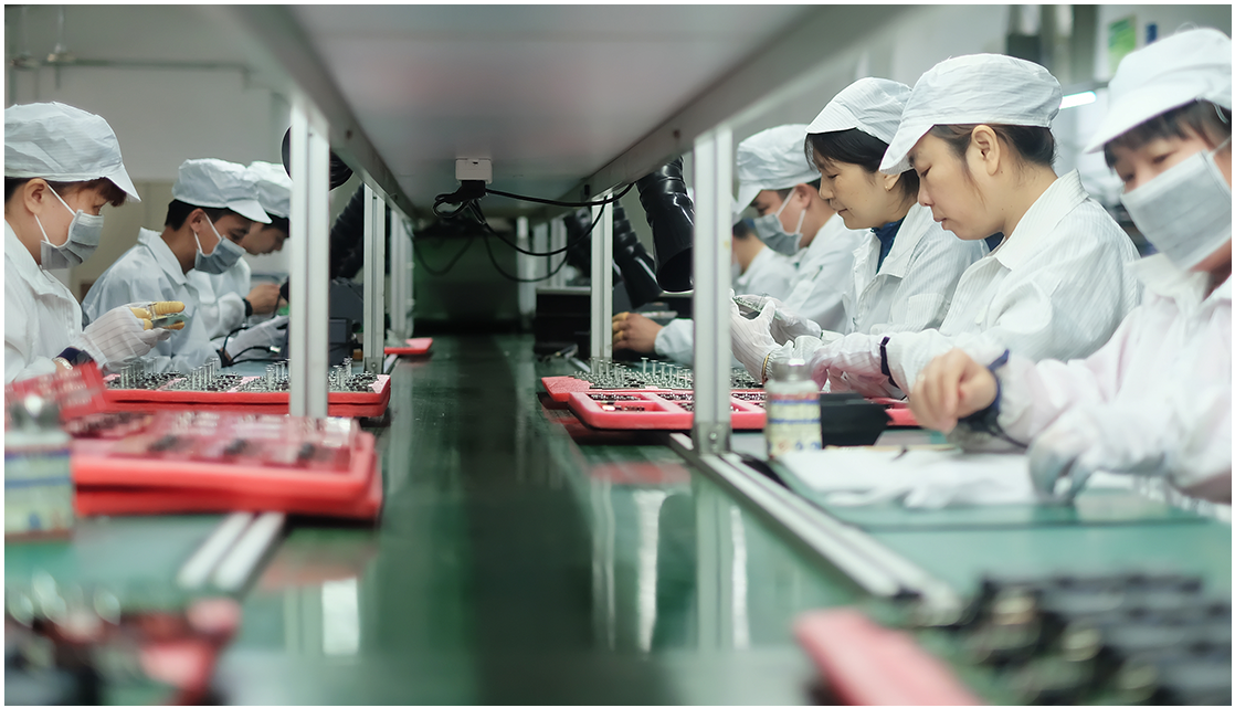
THT Components: Selective Soldering
Through hole components can be either soldered by hand by one of our very experienced operators or using our selective soldering machine. And although manual soldering may seem outdated it is still a useful solution for some components.
In most of the cases we use a selective soldering machine as the process is more reliable. It consists of 3 main steps, the application of liquid flux, preheating of the board, and soldering with a specific solder nozzle.
Last, but not least comes the cleaning, final inspection and the shipping of the assembled board. During final inspection we compare the assembled board to the Visualizer to check the details of order.


 Quote
Quote