Are you creating a new printed circuit board design? Printed circuit boards have many technical uses. However, it is more cost-effective to conduct a concept test before entering the PCB manufacturing stage. The PCB prototype allows the idea to be approved in a cheaper way before the full printed version is manufactured. Even if you may feel that you know exactly how to design a PCB, you must first have a PCB prototype.
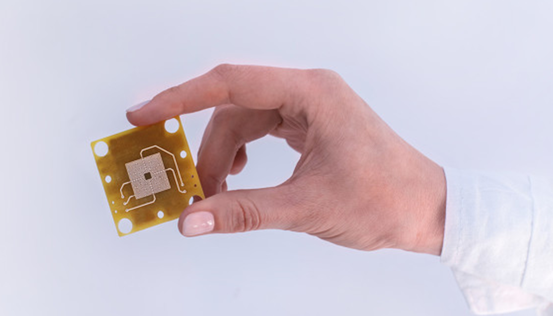
Typical PCB prototype
The two primary stages in developing products such as electronic circuit boards are simulation and prototyping. Although sometimes overlooked, it is done through software, and its purpose is to verify whether the circuit design meets its performance and functional design criteria. An electronic circuit simulation is a valuable tool as it reduces the need to build unnecessary boards that have little chance of meeting design goals. Passing the simulation test is only the first step in electronic design, as the hardware device or PCB must also be tested. Such tests, called PCB prototypes, can be defined by their purpose, process, and result.
1. Purpose
The purpose of PCB prototype is to build and test its functionality, operation, and physical implementation of the design, as well as its structural integrity. Structural integrity refers to the quality and reliability of the PCB, which is usually regulated according to its intended use.
2. Process
PCB prototyping is usually divided into three stages. In the same way that several simulations are required before final parameters are determined and requirements are met, prototyping is cyclical and usually requires several iterations before the final PCB construction is completed.
3. Result
For each PCB prototype iteration, an assembled PCB is created and tested, and the test results determine whether additional iterations are required. Usually, further iterations mean redesigns or design changes and the need to build and test new boards. The result of the PCB prototype is a design that can be used for the PCB, depending on the intended application of the board.
Parallel PCB prototyping
As mentioned above, PCB prototyping is usually an iterative process requiring multiple design changes and rebuilding before the final design is completed, and it is crucial in making your own circuit board. In practice, design quality is proportional to the number of iterations, as each iteration produces a better quality design. Although these cycles can be anticipated, it is usually desirable to keep their number to a minimum. The larger the number of iterations, the more time and cost it takes to develop. However, in most cases, time and cost are limited. For example, most developers have a delivery schedule, which may vary depending on the clients.
Not surprisingly, there are various strategies to reduce lead times, one of which is the use of parallel prototyping strategies. Parallel prototyping can be defined as physically testing different board implementations collectively rather than sequentially, as is done for typical prototypes. Parallelization allows all aspects of the design to be tested or analyzed with a view to improving the overall design more quickly than sequential iterations would allow. There are many measures to improve the effectiveness of parallel prototyping when it is implemented, which includes using cheaper components, larger boards, or otherwise relaxing board parameters.
These methods may be effective and can be applied in typical prototyping; however, each will need to be determined individually and sequentially to provide an accurate comparison, which will, in effect, extend the prototyping process. However, if these alternative designs are manufactured and tested in a simultaneous or parallel manner, they can make the prototyping process more efficient. In these cases, parallel PCB prototyping offers clear advantages.
Parallel prototyping allows the development of a single design to make a single layer board or multiple competing designs to make a multi layer board, which meets the design objectives. In fact, because board manufacturing must be stopped until testing and redesign is completed, the typical process can only be as fast as parallel processing. For parallel prototypes, alternative designs can be manufactured during this downtime, which will significantly increase efficiency.
Clearly, learning from software development and establishing a parallel prototyping strategy can be very beneficial in improving PCB development, but to take full advantage of this approach, manufacturers should have an agile manufacturing process and be able to respond quickly to changes in board design.


 Quote
Quote