Printed circuit boards serve as the backbone of all modern electronic devices. A PCB board serves two important functions in an electronic circuit – (1) mechanical support for circuit components (2) electrical interconnection of electronic components. Whether it is mobile phones, laptops, or LCDs, it is impossible to find an electronic gadget that doesn’t have a PCB.
Types of PCB
Printed circuit boards are getting increasingly complex with advancements in electronics technology. Depending on the target application, PCB boards can be of different types:
- Single-layer PCB
- Double-sided PCB
- Multilayer PCB
- Rigid PCB
- Rigid-flexible PCB
Single-sided PCB
Single-sided PCB boards are the simplest type of circuit board. These printed circuit boards are used for low-density designs. The designing and manufacturing process of single-sided PCBs is simpler as compared to other types of circuit boards. These PCBs are highly cost-effective and easier to troubleshoot. Common applications of single-sided PCB include power supplies, timers, relays, LED circuits, and vending machines.
Double-sided PCB
Double-sided circuit boards consist of a single substrate layer with conductive layers and solder mask on both sides.. Circuit components can be placed on both sides of the PCB. Due to more efficient routing, double-sided PCB boards are the most popular in the electronics manufacturing industry. Double-sided boards have an increased circuit density and design complexity as compared to single-sided circuit boards. Some prominent applications of double-sided PCB boards include power converters, industrial controls, UPS systems, HVAC systems, and automotive circuits.
Multilayer PCB
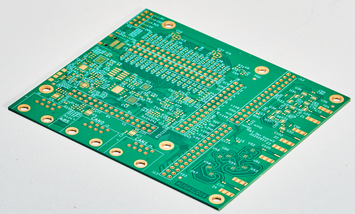
Any PCB board having more than three layers of conductive material is categorized as a multilayer PCB. These different conductive layers are interconnected through copper-plated holes. Multilayer PCB boards are more complex than single and double-sided boards. While the circuit components are placed on the surface layers, inner conductive layers are mostly used for routing. Multilayer PCBs offer the advantages of reduced board size, high circuit density, and greater flexibility. Major downsides of multilayer PCB boards include higher production cost, complex design process, and difficult troubleshooting. Some of the salient applications of multilayer PCB boards are mobile phones, computers, servers, telecommunication equipment, military equipment, and aerospace equipment.
Rigid, Flex, and Rigid-Flex Circuit Boards
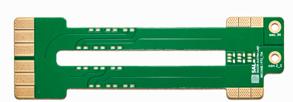
Commonly used PCB boards are made from rigid materials that cannot be bent or folded. However, with the advancement in PCB technology, flexible PCB boards are now available that can be bent and folded. Flexible PCBs are costlier as compared to rigid circuit boards. Nonetheless, flex boards offer many advantages over rigid boards such as flexibility, durability, and connectivity. Flexible circuit boards are especially well suited for wearable electronics and other space-constrained applications.
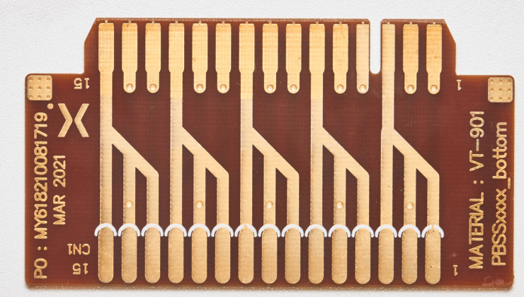
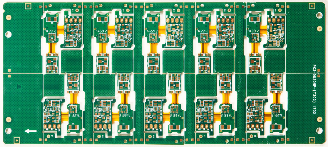
Rigid-flex PCBs are a new class of printed circuit boards that combine the best features of rigid and flex circuit boards. Rigid-flex PCBs combine the flexibility and versatility of flex PCBs with the stability and strength of rigid PCBs. Rigid-flex PCB boards allow the designers to eliminate cables, connectors, and wires. This elimination of external connectors leads to improved performance, reliability, and efficiency. Due to their higher cost, rigid-flex PCB boards are primarily used in high-density and high-reliability applications.
PCB Manufacturing Process
PCB manufacturing is a complex process that requires multiple steps. The complexity of the production process also depends on the type of PCB and the number of layers. From design to fabrication, The PCB manufacturing process relies heavily on CAD/CAM software and automatic machines.
Designing: The first step in the PCB fabrication process is PCB designing. During this process step, engineers design the PCB layout using CAD software packages such as Eagle, Altium Designer, and EasyEDA.
Printing: After the finalization of PCB design, it is sent to a plotter printer that prints the design on transparent films. Separate printouts are created for each layer of the PCB. A registration hole is punched into the films for proper alignment during the production process.
Printing Copper for Internal Layers: The PCB design printed on the laminate is pre-bonded to the copper. The copper is then etched to reveal the PCB design. Next up, the laminate is covered with the resist which is essentially a photo-sensitive film. This resist layer gets hardened when exposed to ultraviolet light.
Etching the Internal Layers: During this process step, the copper traces are covered while the remaining copper is removed using a chemical solution.
Layer Alignment: Optical inspection and layer alignment are performed during this step. The registration hole punched earlier is used for the alignment of internal and external layers. Errors and defects in the board design are detected by the optical inspection machine.
Lamination: After optical inspection, different PCB layers are fused into a single unit. The external layer of the PCB is made of fiberglass coated with epoxy resin. All the layers of the PCB are pressed together using a mechanical press.
Drilling: An X-ray machine is used for determining the drill spots on the PCB. The drilling process is carried out by computerized drilling machines.
Plating: During this process step, the PCB is bathed in different chemicals. A thin layer of copper is deposited on the top layers as well as on the walls of drilled holes.
Solder Masking: In the final step of PCB fabrication, solder mask is applied to the external layers of the PCB board. Ultraviolet light is used for the removal of excess solder mask. The circuit boards are then cured in a specialized oven which helps in preventing corrosion and oxidation.
Shipment: After the completion of fabrication process, the boards are labeled, packed, and shipped off to the customers.
Conclusion
PCB manufacturing technology has advanced significantly in recent decades. Depending on the target application, the type and material of PCB boards vary. Single-sided PCB boards are used for simple applications while double-sided and multilayer PCBs are used for complex applications. With flexible and rigid-flex PCBs it is now possible to create circuit boards that can bend and fold.
Shenzhen Omni PCB is a market leader in PCB manufacturing for over 30 years. We provide the highest quality PCB products in the shortest time possible. Our advanced technology, strict quality control, and excellent customer service set us apart from the competition.


 Quote
Quote