


+86 13603063656
At its core, Surface Treatment in PCB manufacturing refers to the application of a protective and solderable finish on exposed copper areas after etching and before assembly. Copper, though an excellent electrical conductor, is highly susceptible to oxidation when exposed to air and humidity. Even a thin oxide layer can inhibit solder wetting, disrupt current flow, and weaken mechanical bonding. Therefore, Surface Treatment serves two principal functions:
Protect the copper surface from oxidation and contamination during storage and handling.
Provide a solderable surface that ensures consistent interconnection during component assembly.
In modern PCB fabrication, Surface Treatment is not simply a coating. It’s a chemically engineered interface that must adhere precisely to the copper while remaining compatible with subsequent solder reflow and assembly processes. The thickness, composition, and uniformity of this layer determine not only solder joint reliability but also signal transmission quality, especially for high-speed designs.
There are multiple methods to achieve effective Surface Treatment, each based on different metallurgical or chemical principles. Some treatments — such as HASL (Hot Air Solder Leveling) — physically coat the copper with molten solder, while others — like ENIG (Electroless Nickel Immersion Gold) — use a series of autocatalytic reactions to deposit layered metallic finishes. Still others, like OSP, rely on organic compounds that form ultra-thin, temporary protective films.
Thus, the definition of Surface Treatment extends beyond surface protection. It encapsulates the broader challenge of maintaining interconnect reliability throughout the product lifecycle — from the assembly line to field deployment in demanding conditions.

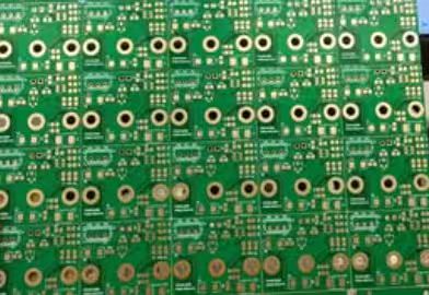
Surface Treatment
Surface Treatment involves a combination of electrochemical and physical processes. The copper surface must first be cleaned and activated to remove oxides, residues, and microscopic contaminants. This is followed by a reaction stage, where the chosen treatment material bonds or deposits onto the copper. For example, in ENIG, nickel is first deposited electrolessly to serve as a diffusion barrier, followed by a thin gold layer that prevents nickel oxidation and provides excellent solderability.
At a microscopic level, Surface Treatment alters surface energy and wettability — critical parameters in achieving reliable solder joints. High surface energy enhances solder spread, while poor surface preparation can lead to incomplete wetting, void formation, or “black pad” defects. Engineers must, therefore, control not only chemical concentration and temperature but also surface roughness and micro-topography during treatment.
In high-frequency PCBs, where signal integrity depends on the uniformity of conductor geometry, even the micro-thickness of the treatment layer becomes significant. Variations in coating thickness can alter impedance values, cause reflection losses, or contribute to insertion loss. As a result, the definition of Surface Treatment extends deeply into the realm of precision engineering.
The history of PCB Surface Treatment mirrors the evolution of electronic complexity. Early PCBs used bare copper, protected only by solder mask, but corrosion and poor solderability quickly made this impractical. The introduction of HASL in the 1970s revolutionized the industry by providing a reliable, low-cost solder coating. However, as component sizes shrank and surface-mount technology (SMT) advanced, the uneven surface of HASL became a problem for fine-pitch components.
This led to the rise of ENIG, which offered exceptional planarity, corrosion resistance, and solderability, making it ideal for high-density designs. Later innovations, such as ENEPIG (Electroless Nickel Electroless Palladium Immersion Gold), further improved contact reliability for gold wire bonding applications.
In parallel, OSP emerged as an eco-friendly, low-cost solution suitable for single-use soldering operations. Although OSP lacks the durability of metal coatings, it became popular for consumer electronics due to its simplicity and compliance with RoHS (Restriction of Hazardous Substances) regulations.
Today, the choice of Surface Treatment is no longer dictated by a single factor like cost or appearance. Instead, it’s a multivariable optimization problem, balancing thermal stability, assembly process compatibility, electrical performance, and long-term reliability.
In my professional view, Surface Treatment symbolizes the intersection of material science, process engineering, and system reliability. While the substrate and copper layers form the body of a PCB, the surface finish acts as its skin — sensitive, protective, and vital. Any flaw in this layer can propagate catastrophic failures during assembly or service life.
The future of Surface Treatment lies in nanostructured coatings, self-healing chemistries, and AI-driven process control. We are entering an era where surface engineering will move beyond passive protection to active functionality — potentially enabling self-soldering, anti-bacterial, or thermal-regulating surfaces.
Manufacturers like JM PCB have already begun integrating precision-controlled Surface Treatment lines with in-line analytical monitoring, ensuring every board achieves uniform coating integrity. This combination of automation and chemistry marks the dawn of a new generation of reliability in PCB manufacturing.
The effectiveness of any Surface Treatment depends heavily on its compatibility with the underlying materials. BT Epoxy Resin, for instance, is widely used in high-performance multilayer boards due to its superior thermal and mechanical stability. However, the chemical composition of BT resin surfaces can influence how metal finishes bond during plating or immersion.
An improper match between resin chemistry and surface finish process can result in adhesion failure, interlayer delamination, or underplating corrosion. Therefore, when engineers design stack-ups involving BT Epoxy Resin, they must select Surface Treatment types that maintain integrity under both thermal cycling and reflow stress.
This underscores the broader engineering truth: Surface Treatment selection is not an isolated decision — it must harmonize with resin systems, copper foils, and assembly conditions.
In the overall flow of PCB fabrication, Surface Treatment occupies a critical stage that bridges the end of copper patterning and the beginning of final inspection and assembly. After the outer copper layers are etched to form conductive traces, the exposed copper pads must be protected before the solder mask and component assembly stages. This is where the chosen Surface Treatment is applied to ensure both oxidation resistance and solderability.
The timing of this process is crucial. If applied too early, contamination or oxidation can compromise the coating’s effectiveness. If applied too late, the copper surface might already exhibit micro-oxidation that reduces bonding quality. High-end manufacturers such as JM PCB have mastered this timing through automated process control systems that track humidity, temperature, and chemical concentration in real time.
In essence, the Surface Treatment step functions as the final metallurgical handshake between the PCB’s conductive network and the external world of components and connectors. Every subsequent solder joint and every mechanical interface relies on its integrity.
The success of any Surface Treatment depends not only on chemistry but also on the environmental control within the fabrication facility. Airborne contaminants, humidity, and residual chemicals from previous process stages can all affect coating uniformity and adhesion.
For example, ENIG requires precise bath chemistry to maintain a consistent nickel-to-gold ratio. Even slight deviations can cause gold layer porosity or nickel hyper-corrosion — leading to the infamous “black pad” defect. In contrast, OSP processes are more forgiving but must be executed under cleanroom conditions to prevent organic contamination that might inhibit solder wetting.
Surface Treatment lines, especially those used for high-end aerospace and automotive PCBs, often operate in controlled micro-environments with automated replenishment systems. The use of inline X-ray fluorescence (XRF) analysis ensures coating thickness and elemental uniformity, providing measurable data for quality assurance.
In my observation, the manufacturing environment surrounding Surface Treatment is as important as the chemical formulation itself. Precision chemistry without precision control is merely a recipe for inconsistency.
PCB designers cannot ignore the implications of Surface Treatment when developing layouts. Certain finishes, like HASL, create non-planar surfaces due to solder deposition. This can interfere with fine-pitch components or BGAs where coplanarity is essential. ENIG, on the other hand, provides an exceptionally flat surface, making it the preferred choice for HDI (High-Density Interconnect) applications.
Designers must also account for thermal conductivity and contact resistance. For instance, immersion silver provides low contact resistance but may tarnish under high humidity. OSP is inexpensive but not suitable for multiple solder reflow cycles.
By anticipating the downstream effects of Surface Treatment early in the design phase, engineers can avoid costly rework or assembly failures. This integration of design-for-surface-finish (DFS) thinking is rapidly becoming standard practice in leading PCB companies.
HASL is one of the oldest and most established Surface Treatment methods. The process involves dipping the PCB into molten solder and then using high-pressure hot air to remove excess solder, leaving a thin, uniform coating on the exposed copper pads.
Advantages:
Excellent protection against oxidation.
Strong, durable solder layer.
Cost-effective for through-hole and large-pitch applications.
Disadvantages:
Uneven surface not ideal for SMT and fine-pitch designs.
Potential for thermal stress due to high processing temperature.
Limited compatibility with lead-free requirements unless special alloys are used.
While HASL remains popular for industrial-grade and consumer electronics, its role is diminishing in fine-line, high-speed, and HDI circuits that demand planarity and tighter tolerances.
ENIG represents a significant advancement in Surface Treatment engineering. The process deposits a nickel layer that acts as a diffusion barrier, followed by a thin gold layer that protects the nickel from oxidation and provides excellent solderability.
Advantages:
Exceptional flatness and planarity.
Ideal for wire bonding and fine-pitch components.
Strong corrosion resistance and mechanical integrity.
Reliable for multiple reflow cycles.
Disadvantages:
Higher cost compared to HASL or OSP.
Requires precise control to prevent “black pad” formation.
Involves more complex chemical management.
ENIG has become the de facto standard for high-end PCB applications, especially in aerospace, telecommunications, and medical devices. It represents the perfect balance between aesthetics, functionality, and reliability.
The ENEPIG Surface Treatment adds a palladium layer between nickel and gold. Palladium acts as an additional diffusion barrier, enhancing wire bond reliability and mitigating the “black pad” issue.
Advantages:
Supports both soldering and gold wire bonding.
Superior corrosion and oxidation resistance.
Improved reliability under high-temperature storage.
Disadvantages:
More expensive due to palladium cost.
Requires more precise chemical control.
ENEPIG is often referred to as the “universal finish” due to its broad compatibility and reliability. It’s increasingly chosen for high-reliability sectors like aerospace electronics and defense systems.
OSP represents the simplest and most environmentally friendly form of Surface Treatment. It applies an organic film — typically based on azole compounds — to protect the copper from oxidation.
Advantages:
Low cost and RoHS-compliant.
Excellent for single reflow processes.
Smooth, planar surface for SMT.
Disadvantages:
Limited shelf life.
Not suitable for multiple solder cycles.
Requires careful storage to prevent oxidation.
OSP is widely used in high-volume consumer electronics where cost efficiency outweighs long-term durability requirements.
Both Immersion Silver and Immersion Tin offer thin metallic coatings that preserve copper and enhance solderability.
- Immersion Silver provides excellent electrical conductivity and is favored for RF and microwave circuits. However, it is prone to tarnish and requires anti-tarnish packaging.
- Immersion Tin offers good solderability but may suffer from tin whisker formation if not properly controlled.
These finishes are often chosen for specific niche applications where electrical performance or cost plays a dominant role.
Every Surface Treatment technique embodies a trade-off between cost, performance, and durability. The challenge for engineers and procurement managers is to determine the “sweet spot” that delivers acceptable performance without unnecessary expense.
- HASL is inexpensive but unsuitable for high-density designs.
- ENIG offers superb quality but comes with higher material and process costs.
- OSP is cost-efficient but limited in durability.
- ENEPIG provides maximum reliability at the highest price point.
This cost-performance dynamic is especially critical in mass production. In consumer devices, where product lifecycles are short, lower-cost treatments like OSP may suffice. But in aerospace or medical devices, reliability failures can lead to catastrophic consequences, justifying premium finishes.
A significant variable in the overall cost of a high-performance PCB lies in the choice of BT Epoxy Resin, the preferred substrate for advanced multilayer boards. BT resin offers exceptional thermal stability, dimensional control, and low dielectric loss, making it ideal for high-frequency and high-speed circuits.
However, these advantages come with higher material and processing costs. BT resins typically require higher lamination temperatures, longer curing cycles, and precise adhesion control, all of which increase production complexity. Additionally, certain Surface Treatment chemistries must be adjusted to ensure reliable adhesion to BT-based substrates.
For instance, ENIG coatings require careful surface activation when applied over BT epoxy-based laminates to ensure uniform nickel deposition. Failure to do so can lead to poor interface adhesion or voiding. As a result, the total cost of a BT epoxy-based PCB is influenced not only by resin price but also by Surface Treatment process optimization.
From my engineering perspective, BT Epoxy Resin represents a material where cost is directly proportional to performance — its robustness justifies its price, especially when paired with high-quality finishes such as ENIG or ENEPIG.
When evaluating Surface Treatment costs, engineers should move beyond per-board pricing and consider total cost of ownership (TCO). This includes:
Yield rates and rework reduction.
Shelf life and handling sensitivity.
Field failure rates and warranty claims.
A low-cost finish that results in high defect rates ultimately proves more expensive than a premium alternative that ensures near-zero failures. For example, ENEPIG may increase production costs by 15%, but if it prevents even a small percentage of field failures in mission-critical applications, the return on investment is substantial.
Thus, the real measure of cost efficiency in Surface Treatment lies in long-term reliability, not immediate savings. Manufacturers who understand this principle achieve both operational excellence and customer trust.
| Surface Treatment Type | Cost Level | Flatness | Shelf Life | Solderability | Lead-Free | Typical Applications |
|---|---|---|---|---|---|---|
| HASL | Low | Medium | Medium | Good | Optional | General electronics |
| Lead-Free HASL | Medium | Medium | Medium | Good | Yes | Automotive, consumer |
| OSP | Very Low | Excellent | Short | Excellent | Yes | Consumer electronics |
| ENIG | High | Excellent | Long | Excellent | Yes | Aerospace, medical |
| ENEPIG | Very High | Excellent | Very Long | Excellent | Yes | Medical, defense |
| Immersion Silver | Medium | Excellent | Medium | Excellent | Yes | High-speed circuits |
| Immersion Tin | Low | Excellent | Short | Good | Yes | Industrial electronics |
In the rapidly evolving landscape of PCB fabrication, Surface Treatment represents far more than a final coating step—it is the culmination of chemistry, physics, and design intelligence working together to determine how a printed circuit board performs over its lifetime. The journey from raw copper to a functional surface capable of reliable soldering, strong adhesion, and long-term corrosion resistance reflects the technical sophistication of modern electronics manufacturing.
At its core, the selection of Surface Treatment is about achieving harmony between performance requirements, environmental constraints, and economic realities. Each method—whether OSP, ENIG, ENEPIG, immersion silver, or lead-free HASL—embodies a different balance between these factors. For example, OSP is attractive for cost-sensitive consumer electronics, while ENEPIG remains indispensable in aerospace or medical devices, where even a microscopic corrosion layer can lead to mission failure.
A successful PCB is therefore not defined merely by the quality of its traces or the precision of its layers, but by how effectively its surface interacts with the components it supports. A well-chosen Surface Treatment ensures solderability, electrical continuity, and resilience under harsh operating environments. The transition from traditional plating to plasma-enhanced or nano-structured coatings signals a deeper understanding of how surfaces behave at the atomic level—how electrons, moisture, and ions interact in ways that influence the board’s electrical stability and long-term reliability.
Material science continues to shape the frontier of this discipline. BT Epoxy Resin, though more costly than standard FR-4, exemplifies the high-value material choices driving PCB evolution. Its superior thermal and mechanical stability ensures that advanced finishes like ENEPIG can reach their full potential without the substrate becoming a limiting factor. In essence, investing in BT resin and high-quality Surface Treatment is not an expense—it is an assurance of performance continuity in high-stress, high-speed environments.
As we look to the future, sustainability and digitalization will increasingly define the direction of Surface Treatment innovation. The industry is already moving toward lead-free, cyanide-free, and low-emission processes, supported by AI-driven bath management and predictive quality control. The rise of digital twins and process automation allows manufacturers to anticipate failure points and optimize coating parameters before the first board even enters production. This integration of data and chemistry represents the next evolutionary step in surface engineering.
However, even as technology advances, craftsmanship remains irreplaceable. The intuition of skilled engineers, their ability to sense subtle process variations, and their understanding of how microscopic changes translate into macroscopic reliability—all of these remain the heart of PCB excellence. Machines can measure and optimize, but only human insight can innovate and adapt.
1. How do manufacturers ensure the consistency of Surface Treatment quality?
Manufacturers employ automated plating lines, in-line thickness measurement, and cross-sectional analysis under IPC standards. Continuous monitoring of bath chemistry and temperature ensures repeatable coating quality.
2. Why is ENEPIG considered superior to ENIG in certain applications?
ENEPIG adds a palladium barrier between nickel and gold, preventing corrosion and ensuring stable solderability even after long storage periods, making it ideal for medical and aerospace electronics.
3. How does BT Epoxy Resin affect PCB performance?
BT Epoxy Resin offers high glass transition temperature (Tg), mechanical stability, and low moisture absorption. Although it raises material costs, it significantly enhances thermal reliability and solder joint integrity.
4. What are common causes of oxidation in Surface Treatment processes?
Oxidation occurs due to improper rinsing, residual contaminants, or prolonged air exposure. Using nitrogen drying and maintaining cleanroom environments can minimize oxidation risk.
5. Which Surface Treatment is best suited for fine-pitch components?
ENIG or ENEPIG is preferred due to their flat, uniform surfaces, which ensure reliable solder joints in BGA and QFN packages.


Connect to a Jerico Multilayer PCB engineer to support your project!
Request A Quote


 Quote
Quote