


+86 13603063656
Printed Circuit Boards (PCBs) form the backbone of modern electronic devices, enabling the interconnection of electronic components while maintaining signal integrity and structural stability. As electronics continue to shrink in size while increasing in functionality, the complexity of PCBs grows, leading to higher demands for precision, reliability, and manufacturability. Among the many design and manufacturing considerations in PCB fabrication, via protection and solder mask integrity are paramount. One crucial process that addresses these challenges is Tenting.
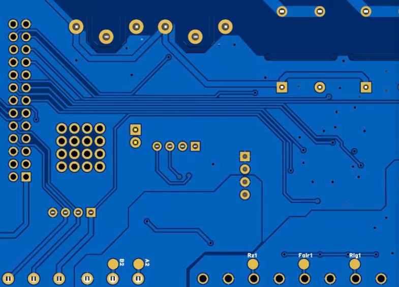
Tenting in PCB manufacturing is a technique where the via, the plated through-hole connecting different layers of the board, is covered or partially covered with solder mask. This simple yet highly effective process serves multiple purposes: it prevents solder from flowing into the via during assembly, protects the via from environmental contaminants such as moisture and dust, and contributes to overall electrical and mechanical reliability. Despite being a relatively straightforward process, the role of Tenting in enhancing PCB performance cannot be overstated.

Tenting
Tenting is a critical process in PCB manufacturing, aimed at protecting vias—the vertical conductive channels that interconnect different layers of a PCB—from environmental and assembly-related risks. Despite its apparent simplicity, Tenting is a sophisticated process that requires precise material selection, careful design, and accurate application during manufacturing.
At its core, Tenting is the application of solder mask over a via to seal or partially cover it. The purpose is to create a protective barrier that prevents solder, dust, moisture, and other contaminants from entering the via. While the via itself is essential for electrical connectivity, its exposure can be a liability if not properly managed. By covering the via with a thin, uniform layer of solder mask, tenting preserves both the electrical functionality and structural integrity of the PCB.
Technically, tenting is considered a masking process, where the solder mask acts as both a protective coating and an insulator. Depending on the manufacturing requirements, Tenting can be:
Fully Tented: The via is completely covered on one or both sides of the PCB. This ensures maximum protection against solder intrusion and environmental contaminants.
Partially Tented (Plugged or Capped): Only a portion of the via opening is covered. This method balances protection with cost and allows for certain assembly or thermal considerations.
Untented: The via remains open, either intentionally for electrical or thermal reasons, or due to design constraints. While this approach reduces material usage and process steps, it exposes the via to potential defects.
The selection between these methods depends on the board’s complexity, intended application, and environmental conditions. High-reliability boards often mandate fully tented vias, while lower-cost consumer electronics may allow partially tented or untented vias.
Several techniques exist to achieve Tenting in PCB manufacturing, each offering specific advantages and challenges:
Photoimageable Solder Mask Tenting:
This is the most common method used in modern PCB fabrication. The solder mask is applied as a liquid photoimageable coating, then exposed to ultraviolet (UV) light through a phototool, which defines the areas to remain uncovered. The exposed areas are developed, leaving the solder mask over the vias. This method provides high precision and is suitable for small vias in high-density boards.
Dry Film Tenting:
In this technique, a pre-cured dry film solder mask is laminated onto the PCB. The via openings are then exposed and developed, similar to photoimageable methods. Dry film tenting offers excellent uniformity and can handle thicker solder mask layers, making it useful for high-reliability or heavy copper boards.
Mechanical Plugging or Filling with Solder Mask:
This method physically fills the via with solder mask material before curing. It is often used in conjunction with photoimageable or dry film methods to reinforce the via seal. Mechanical plugging is particularly effective for vias exposed to high thermal or mechanical stress.
Each of these techniques must be carefully controlled to ensure that the solder mask completely covers the via without voids, bubbles, or insufficient adhesion. Any defect in the tenting process can compromise the via’s protection, leading to solder wicking, oxidation, or mechanical failure.
Understanding the distinctions between tented, partially tented, and untented vias is crucial for PCB designers and manufacturers:
Tented Vias: Provide full coverage, ensuring maximum protection. They are ideal for high-density boards, high-frequency applications, and harsh environments. The solder mask fully seals the via opening, preventing solder or contaminants from entering.
Partially Tented Vias: Cover only part of the via, usually on the top side. They reduce material usage and process complexity but offer less protection. Partially tented vias may still require additional process controls during assembly to prevent defects.
Untented Vias: Remain open and are exposed. They are typically used for thermal vias, where direct contact with solder or copper planes is necessary to dissipate heat. Untented vias, however, are vulnerable to solder wicking, contamination, and environmental degradation.
The choice among these approaches depends on balancing protection, performance, manufacturability, and cost. High-reliability applications, such as medical electronics or aerospace boards, usually prioritize fully tented vias to minimize risks, while consumer electronics may accept partially tented vias to reduce cost.
Tenting directly contributes to the long-term reliability of PCBs. By sealing vias, it prevents the ingress of moisture and dust, which can cause corrosion, short circuits, or impedance variations. Tented vias also reduce the likelihood of solder bridging during assembly, improving manufacturing yield and consistency.
Moreover, in high-speed or high-frequency applications, tented vias help maintain signal integrity. Open vias can act as parasitic elements, creating unwanted capacitance or inductance that distorts signal propagation. By carefully applying solder mask during tenting, designers can minimize these parasitic effects and ensure consistent electrical performance.
Tenting in PCB manufacturing is more than just covering vias with solder mask—it is a carefully engineered process that directly affects board performance, reliability, and manufacturability. The design principles behind Tenting influence everything from mechanical stability to electrical signal integrity. Understanding these principles is essential for PCB designers, fabrication engineers, and quality control specialists.
The effectiveness of Tenting depends on several design parameters that must be carefully optimized during the PCB design and manufacturing process:
Via Size and Aspect Ratio:
The diameter and depth of the via are critical factors in determining how effectively it can be tented. Small vias or microvias may be fully covered with minimal solder mask thickness, while larger vias may require multiple process steps to ensure complete coverage. The aspect ratio (depth-to-diameter ratio) affects solder mask adhesion and the risk of void formation.
Pad-to-Via Relationship:
The size of the annular ring around the via pad affects solder mask coverage and mechanical stability. Adequate pad size ensures that the solder mask adheres properly and that the via remains sealed during thermal cycling. Poorly sized pads can lead to mask lifting, cracking, or incomplete tenting.
Solder Mask Thickness:
The solder mask must be thick enough to completely cover the via without introducing stress or defects. Excessive thickness can create mechanical stress or interfere with component placement, while insufficient thickness may result in incomplete tenting.
Via Density and Board Layout:
High via density in multilayer or HDI boards presents challenges for tenting, as overlapping vias can make solder mask application more complex. Designers must consider spacing and layout rules to ensure proper coverage while minimizing mask defects.
Thermal Considerations:
Boards subjected to high thermal cycling or assembly processes such as reflow soldering must account for solder mask expansion, contraction, and adhesion. Proper tenting design mitigates the risk of mask cracking or peeling under thermal stress.
Tented vias play a significant role in maintaining electrical performance, especially in high-frequency and high-speed circuits. The following aspects illustrate the relationship between tenting and electrical characteristics:
Signal Integrity:
Open vias can act as parasitic elements, introducing unwanted capacitance and inductance that distort signal propagation. Tented vias reduce these parasitic effects, helping maintain consistent impedance and minimizing signal reflection.
Crosstalk Reduction:
In high-density boards, closely spaced vias can induce electromagnetic coupling. Tenting provides a dielectric barrier that mitigates crosstalk between adjacent vias and traces.
Controlled Impedance:
By sealing vias with a uniform solder mask layer, designers can better control impedance across the PCB, which is essential for RF, high-speed digital, and high-frequency analog applications.
The mechanical performance of a PCB is also influenced by tenting:
Structural Stability:
The solder mask acts as a mechanical reinforcement over vias, reducing the likelihood of via collapse or cracking during handling and assembly. Fully tented vias improve overall board rigidity, which is particularly important for multilayer and flexible PCBs.
Thermal Management:
Tented vias help in managing thermal stress by preventing solder from entering the via, which can create hotspots or uneven thermal expansion. Properly tented vias ensure that the board can withstand repeated thermal cycles without degradation.
Environmental Protection:
Tenting shields the via from moisture, dust, and other contaminants that could compromise mechanical and electrical performance. This is critical for boards used in harsh environments, such as automotive or aerospace applications.
Signal integrity and long-term reliability are tightly linked to Tenting design:
High-Frequency Performance: In RF and microwave circuits, even minor via exposure can create impedance discontinuities that lead to signal loss or reflection. Tenting provides a controlled dielectric environment around the via, reducing signal distortion.
Long-Term Reliability: Sealed vias prevent corrosion, oxidation, and solder wicking, extending the operational lifespan of the PCB. Tented vias are particularly beneficial in boards that will experience frequent thermal cycling or high-humidity conditions.
Assembly Yield: By reducing solder bridging and other via-related defects, tenting improves the overall yield of PCB assembly. Boards with well-designed tenting are less likely to require rework or experience failures during testing.
Based on experience and industry best practices, several recommendations can optimize Tenting performance:
Collaborate with Fabricators Early: Discuss via size, density, and tenting requirements with your PCB manufacturer, such as JM PCB, to ensure manufacturability and reliability.
Use Appropriate Solder Mask Materials: Select solder masks with proven adhesion, thermal stability, and dielectric properties suitable for your application.
Simulate Electrical Effects: For high-speed or high-frequency boards, simulate the impact of tented vias on impedance, signal reflection, and crosstalk before finalizing the design.
Test Prototypes: Conduct thorough electrical, thermal, and mechanical testing on prototypes to validate tenting performance, especially for critical applications.
Consider Via Filling for Extreme Conditions: In boards subject to severe thermal or mechanical stress, combining tenting with via filling (with epoxy or conductive material) can enhance performance and reliability.
The success of Tenting in PCB manufacturing depends heavily on the materials used and how they are applied. The solder mask, which forms the barrier over the via, must meet stringent requirements for adhesion, thermal stability, chemical resistance, and dielectric performance. Selecting the right materials ensures that tented vias perform reliably under both assembly and operational conditions.
Solder mask materials can generally be divided into liquid photoimageable (LPI) masks, dry film masks, and specialized high-performance resins. Each type has its advantages and is chosen based on the specific demands of the PCB design and application:
Liquid Photoimageable (LPI) Solder Masks:
LPI masks are widely used due to their precision, flexibility, and ease of application. They are applied as a liquid coating, exposed through a phototool, and then developed to cover the vias. LPI solder masks provide:
High-resolution coverage for fine-pitch boards
Excellent adhesion to copper and dielectric substrates
Uniform thickness, essential for consistent tenting performance
Dry Film Solder Masks:
Dry film masks are laminated onto the PCB and offer high uniformity in thickness and coverage. These masks are particularly useful for high-reliability or heavy copper boards, where thicker layers of solder mask are required. Dry film masks provide:
Superior mechanical reinforcement over vias
Reduced risk of voids or incomplete coverage
Stable performance under thermal cycling
Specialty High-Performance Resins:
For extreme environments, such as aerospace or automotive applications, specialty resins may be used to provide enhanced thermal resistance, chemical stability, or dielectric performance. These resins ensure that tented vias remain intact even under severe operational stress.
Several material properties directly impact the effectiveness and reliability of tented vias:
Adhesion: The solder mask must adhere strongly to the copper pad and surrounding substrate to prevent lifting or peeling. Poor adhesion is a leading cause of tenting failure.
Thermal Stability: The solder mask must withstand reflow soldering temperatures, thermal cycling, and operational heat without cracking or delaminating.
Chemical Resistance: Solder masks should resist flux, cleaning agents, and environmental contaminants that could degrade the tented via.
Dielectric Strength: A strong dielectric barrier ensures that the tented via does not introduce unwanted electrical leakage or capacitance, which could affect high-speed circuits.
Flexibility: Especially for rigid-flex boards, the solder mask must accommodate bending and flexing without cracking or detaching.
Selecting the appropriate solder mask is a critical design decision. Factors to consider include:
Board Complexity: High-density and multilayer PCBs require solder masks that can maintain precise coverage over microvias and tented vias without causing bridging or voids.
Operational Environment: PCBs exposed to harsh conditions—high humidity, vibration, or extreme temperatures—benefit from high-performance resins or dry film masks.
Assembly Process: Wave soldering, reflow soldering, and selective soldering processes impose different stresses on solder masks. The mask must be compatible with the chosen assembly method.
Signal Requirements: For high-frequency or RF boards, the dielectric constant and uniformity of the solder mask affect signal integrity. Material selection must consider these electrical properties.
By carefully matching solder mask properties to PCB requirements, designers can ensure that tented vias provide reliable protection, maintain signal performance, and enhance long-term board reliability.
Tenting is a versatile process applied across a wide range of PCB types. The method, materials, and design considerations vary depending on board construction, via density, and operational requirements. Understanding these differences is essential for achieving high reliability, manufacturability, and electrical performance.
Rigid PCBs are the most common type of boards used in electronics, providing structural stability and supporting dense component placement. In rigid PCBs, tenting serves primarily to:
Prevent solder wicking during assembly
Protect vias from moisture and dust
Maintain consistent electrical performance across layers
For flexible PCBs, which bend or fold in devices such as wearables, medical sensors, and foldable displays, tenting must also account for mechanical stress. The solder mask used in tenting flexible PCBs must be highly adhesive, flexible, and resistant to cracking. Improperly tented vias in flexible boards can lead to micro-cracks or delamination when the board is flexed repeatedly.
HDI PCBs feature microvias, fine traces, and high via density, making Tenting both more challenging and more critical. The small size of microvias increases the risk of incomplete coverage or void formation during the tenting process. However, effective tenting is essential for HDI boards to:
Preserve signal integrity for high-speed digital and RF applications
Prevent solder bridging in dense layouts
Enhance thermal management by controlling solder flow
Advanced tenting techniques, such as photoimageable masks with controlled thickness, are often employed in HDI boards. High-precision application ensures that even microvias are properly sealed, maintaining both electrical and mechanical reliability. For manufacturers seeking expert solutions in HDI tenting, JM PCB provides specialized processes and materials optimized for high-density designs, ensuring defect-free tented vias in complex boards.
Multilayer PCBs, commonly used in computers, servers, and advanced electronics, contain multiple stacked layers of copper and dielectric materials. Each additional layer increases via density and the complexity of solder mask application. Challenges for tenting in multilayer boards include:
Ensuring uniform coverage across deep vias
Maintaining adhesion under repeated thermal cycling
Avoiding solder mask cracking during lamination and pressing processes
Properly tented vias in multilayer boards contribute to:
Reduced risk of short circuits
Improved long-term reliability under environmental stress
Consistent electrical performance, even in complex high-frequency circuits
Designers often coordinate with fabricators to optimize via-to-pad ratios, mask thickness, and exposure processes to ensure successful t-enting in multilayer boards.
Tenting is applied in a variety of industries, each with specific requirements:
Automotive Electronics: Tented vias protect boards from vibration, heat, and moisture, ensuring reliability in harsh operating conditions.
Medical Devices: High-reliability PCBs in medical equipment demand fully tented vias to prevent contamination and ensure patient safety.
Aerospace and Defense: Extreme environmental conditions and strict regulatory standards require high-quality tenting to maintain board performance and reliability.
Consumer Electronics: In high-density smartphones, tablets, and wearables, tented vias prevent solder bridging, maintain signal integrity, and support miniaturization.
| Factor | Recommendation |
|---|---|
| Via Type | Fully tented for high-reliability; partially tented for cost-effective designs |
| Via Size & Aspect Ratio | Optimize to ensure solder mask coverage and minimize voids |
| Pad Size | Ensure adequate annular ring for solder mask adhesion |
| Solder Mask Type | LPI for precision; dry film for thicker coverage; specialty resins for extreme environments |
| Electrical Performance | Consider impedance, crosstalk, and signal integrity |
| Mechanical & Thermal Considerations | Choose flexible, adhesive masks for rigid-flex; ensure thermal stability |
| High-Density Applications | Employ precise tenting techniques and consult manufacturers like JM PCB |
| Inspection & Testing | Inspect for voids, mask adhesion, and via coverage; validate reliability |
Tenting in PCB manufacturing is an essential process for via protection, solder mask integrity, and overall board reliability. From high-density HDI boards to flexible and multilayer designs, properly tented vias reduce the risk of solder wicking, contamination, and electrical failures.
The effectiveness of tenting depends on careful design, material selection, and precise manufacturing processes. Key factors include via size, pad design, solder mask type, and application technique. Fully tented vias offer the highest protection, while partially tented vias provide a cost-effective alternative in less critical applications.
In addition to mechanical and environmental protection, tenting enhances signal integrity, minimizes parasitic effects, and supports high-frequency applications. Choosing experienced manufacturers, such as JM PCB, ensures that tenting processes are optimized for quality, yield, and reliability.
Ultimately, tenting may seem like a small step in PCB production, but it has a major impact on performance, manufacturability, and long-term reliability. Integrating tenting considerations early in the design phase ensures that boards meet both functional and environmental requirements, making it a cornerstone of modern PCB engineering.
What considerations should be made when designing tented vias for flexible PCBs?
Flexible PCBs require solder masks with high flexibility and adhesion. Vias should be carefully sized to prevent cracking during bending, and the tenting process must account for repeated mechanical stress.
How does Tenting impact high-frequency signal performance?
Tenting reduces parasitic capacitance and inductance by covering the via with a dielectric solder mask, helping to maintain impedance consistency and minimizing signal reflections.
Can Tenting prevent all types of via defects?
While Tenting protects against solder wicking, contamination, and oxidation, it cannot prevent all defects such as internal via voids or mechanical damage during handling. Proper manufacturing control is still required.
What are the most common causes of Tenting failure?
Common causes include poor solder mask adhesion, insufficient mask thickness, incorrect via-to-pad ratios, and thermal or mechanical stress during assembly.
How does solder mask thickness affect Tenting?
Proper solder mask thickness ensures complete coverage without cracking or delamination. Too thin a layer may result in incomplete protection, while too thick a layer may stress the mask or interfere with component placement.


Connect to a Jerico Multilayer PCB engineer to support your project!
Request A Quote


 Quote
Quote