


+86 13603063656
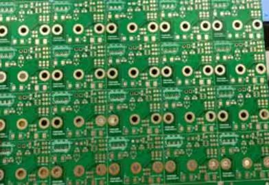
The PCB Plating Process is the controlled deposition of metallic layers on the surface or through the holes of a printed circuit board. This process creates conductive paths, enhances solderability, and protects copper surfaces from oxidation or wear. Fundamentally, plating involves transferring metal ions from a solution (electrolyte) onto the PCB surface through either an electrochemical or chemical (autocatalytic) reaction.
Two broad categories define how plating is achieved:
Electrolytic Plating: Metal ions are deposited by applying an electrical current between an anode (metal source) and the PCB as a cathode. This method allows controlled thickness and uniform coatings but requires electrical connectivity across the plated areas.
Electroless Plating: No external current is applied. Instead, chemical reactions drive the deposition of metals like nickel or copper onto catalyzed surfaces. ENIG, for example, relies on an autocatalytic process for nickel deposition followed by immersion gold replacement.
The essence of the PCB Plating Process lies in its precision. The thickness of each metal layer, typically measured in microns, determines how the board will perform under soldering, thermal cycling, and environmental exposure. For example, ENIG deposits around 3–6 µm of nickel topped with a thin 0.05–0.1 µm layer of gold, whereas hard gold plating may exceed 1 µm in gold thickness for mechanical durability.
In summary, plating transforms bare copper traces into stable, solderable, and reliable interfaces that sustain years of electrical and mechanical stress. It is not merely a finishing touch—it is a functional layer critical to the integrity of the entire electronic assembly.

The PCB Plating Process
Each metallic layer applied during the PCB Plating Process serves multiple purposes, combining chemical protection, electrical enhancement, and mechanical reinforcement.
Key objectives include:
Corrosion Resistance: Copper oxidizes easily, forming non-conductive oxides. Nickel, tin, and gold coatings shield copper from air, humidity, and sulfur compounds.
Solderability Enhancement: The plating layer provides a clean, wettable surface that ensures strong, void-free solder joints during assembly.
Wear Resistance: For connector fingers and contact pads, hard gold plating offers extreme durability, resisting thousands of insertion cycles.
Electrical Conductivity: Smooth plated finishes maintain low contact resistance, crucial for high-frequency and low-loss signal applications.
Thermal Stability: Plating prevents copper migration and intermetallic growth under heat stress, stabilizing joints over long operating lifespans.
Without a properly executed PCB Plating Process, the copper surfaces on a PCB would degrade rapidly, leading to poor solder joints, increased resistance, and premature product failure.
While gold and nickel dominate high-end finishes, other metals play specific roles within the PCB Plating Process ecosystem:
| Metal | Primary Function | Applications |
|---|---|---|
| Nickel (Ni) | Barrier layer preventing copper diffusion | Used under gold in ENIG or hard gold |
| Gold (Au) | Corrosion resistance, contact reliability | ENIG, hard gold, selective gold plating |
| Silver (Ag) | High conductivity, moderate corrosion resistance | Immersion silver finishes |
| Tin (Sn) | Solderability and low cost | Immersion tin and HASL finishes |
| Copper (Cu) | Base conductive layer | Core and through-hole plating |
Each combination yields a unique balance of cost, performance, and process complexity. For instance, ENIG combines nickel’s barrier strength with gold’s chemical stability, while hard gold plating sacrifices some cost efficiency for unmatched durability in contact applications.
A modern PCB Plating Process unfolds through tightly controlled stages:
Surface Cleaning: Mechanical brushing and chemical cleaning remove oxides and contaminants from copper surfaces.
Activation: Surfaces are catalyzed (often using palladium) to initiate uniform deposition.
Nickel Plating (Electroless or Electrolytic): A nickel layer forms as a barrier and bonding interface.
Gold Deposition: Immersion or electrolytic gold is applied for corrosion resistance and conductivity.
Rinsing and Drying: Thorough rinsing removes chemical residues to prevent cross-contamination.
Inspection and Thickness Testing: X-ray fluorescence (XRF) verifies coating uniformity and adherence.
Process control here is crucial. Even slight deviations in bath chemistry or temperature can cause defects such as “black pad” in ENIG plating or non-uniform thickness in electrolytic gold deposition.
The PCB Plating Process landscape encompasses multiple techniques, each designed to achieve specific goals in terms of performance, cost, and manufacturability. The most common methods include:
HASL (Hot Air Solder Leveling) — Traditional solder coating that remains cost-effective but has limitations for fine-pitch designs.
ENIG (Electroless Nickel Immersion Gold) — A two-layer chemical plating that provides excellent solderability and flatness.
Immersion Silver and Immersion Tin — Economical, lead-free finishes that balance performance and affordability.
Hard Gold (Electrolytic Gold over Nickel) — Mechanically robust finish used for contact areas and high-durability connectors.
Each of these approaches within the PCB Plating Process framework has distinct chemical foundations and functional outcomes, shaping how the board behaves under thermal, electrical, and mechanical stress.
The ENIG process—short for Electroless Nickel Immersion Gold—is one of the most widely adopted surface finishes for high-reliability electronics. It involves a dual-layer structure: a nickel barrier layer deposited electrolessly, followed by a thin gold layer applied through immersion replacement.
Key characteristics:
Flat surface profile: Ideal for fine-pitch components and BGA soldering.
Excellent corrosion resistance: Gold prevents oxidation and tarnish.
High solderability: Nickel supports uniform wetting, even after storage.
Good shelf life: ENIG boards remain stable for months without degradation.
Process steps:
Copper surface activation.
Autocatalytic nickel deposition (~3–6 µm).
Immersion gold replacement (~0.05–0.1 µm).
Rinsing, drying, and testing via XRF and solderability analysis.
Advantages:
ENIG is known for its balance between reliability and manufacturability. It provides consistent thickness, smooth topography, and predictable soldering behavior.
Drawbacks:
However, ENIG requires tight process control. Poorly maintained baths can lead to the “black pad” defect—nickel corrosion at the gold interface—reducing joint reliability.
In the context of the PCB Plating Process, ENIG represents a high-precision, chemistry-driven finish suitable for HDI, RF, and fine-pitch assemblies.
The Immersion Silver finish replaces copper atoms with silver through a controlled chemical exchange. It is a cost-effective, lead-free surface treatment suitable for mid-level reliability applications.
Key advantages:
Excellent electrical conductivity.
Flat surface ideal for fine-pitch mounting.
Low cost compared to gold finishes.
Challenges:
Silver tarnishes easily when exposed to sulfur or moisture.
Requires anti-tarnish coatings and sealed storage conditions.
Despite its challenges, immersion silver remains popular in telecommunications and high-speed digital applications where surface smoothness and conductivity outweigh cosmetic concerns.
Immersion Tin plating uses a chemical replacement reaction that deposits tin on copper, forming a Cu–Sn intermetallic compound.
Strengths:
Very cost-effective and fully lead-free.
Good solderability within limited storage duration.
Simple chemistry and equipment requirements.
Limitations:
Tin whisker growth under certain conditions.
Relatively short shelf life.
Not suitable for multiple soldering cycles.
Immersion tin is best suited for consumer electronics or short-lifecycle products where cost efficiency dominates performance priorities.
Hot Air Solder Leveling (HASL) remains a classic PCB Plating Process technique where molten solder is applied to copper pads and leveled with hot air knives.
Benefits:
Low cost and easy reworkability.
Good solder coverage and protection.
Limitations:
Uneven surface unsuitable for fine-pitch components.
Thermal stress during processing.
Environmental concerns with lead-based solder.
Lead-free HASL substitutes tin-copper or tin-silver-copper alloys, mitigating environmental impact but still lacking the smoothness of chemical finishes like ENIG.
The Hard Gold plating technique, also known as Electrolytic Nickel Gold, is the finish of choice when maximum durability is required. Unlike immersion gold, which is thin and chemically deposited, hard gold is electrolytically plated, allowing greater control over thickness—often exceeding 1 µm of gold.
Advantages:
Exceptional wear resistance for connector fingers and edge contacts.
Low contact resistance, even after thousands of mating cycles.
Excellent corrosion protection.
Limitations:
High cost due to gold consumption.
Poor solderability (requires selective plating to avoid solder pads).
Applications:
Edge connectors and switch contacts.
Aerospace and defense electronics.
Industrial control systems.
The PCB Plating Process for hard gold typically involves applying an electrolytic nickel base followed by a hardened gold alloy containing small amounts of cobalt to improve mechanical strength. This finish is not only functional but also symbolic of quality and endurance—often used in mission-critical electronics where replacement is not an option.
One of the most critical performance determinants in a PCB Plating Process is electrical conductivity. Every layer, from nickel to gold, influences the way electrons travel across contacts, vias, and solder joints. The conductivity of the plating metal determines not only how efficiently a signal passes but also how much energy is lost to resistance or heat.
For instance, gold has one of the highest conductivities among metals used in electronics, providing low-resistance paths ideal for high-frequency and RF applications. Nickel, while not as conductive, acts as a diffusion barrier that prevents copper migration—a problem that can cause long-term instability in high-speed designs.
In signal-critical circuits such as 5G modules or radar PCBs, even a minor increase in surface roughness or oxide contamination can cause signal attenuation. That’s why an optimized PCB Plating Process focuses on achieving ultra-smooth and contamination-free finishes, ensuring impedance stability across the operating bandwidth.
Solderability refers to how easily molten solder wets and adheres to a metallic surface. The PCB Plating Process directly dictates this behavior. If a plated layer forms oxides or contaminants, solder may bead up instead of forming a strong joint.
ENIG finishes offer excellent solderability due to gold’s inertness and the smooth nickel surface beneath.
Immersion tin provides good initial solderability but degrades quickly with exposure.
Hard gold is typically not soldered; it’s used in connector applications where wear resistance matters more than solder joint formation.
The surface energy and cleanliness of the plating define wetting quality. Hence, plating chemistry control, rinsing thoroughness, and drying conditions are all critical process factors that determine how well solder bonds during reflow or wave soldering.
Durability is a crucial metric for PCBs used in connectors, switches, or mechanical interfaces. The PCB Plating Process influences hardness, surface texture, and resistance to abrasion.
Hard gold plating, for instance, excels in mechanical endurance. Its structure includes small percentages of cobalt or nickel that harden the gold layer, enabling it to withstand tens of thousands of mating cycles without losing conductivity.
ENIG, on the other hand, is relatively soft due to its thin immersion gold layer. While excellent for soldering, it is not ideal for mechanical contact zones. Engineers often specify selective plating, where hard gold is applied to connectors while ENIG is used on solderable areas—an efficient compromise between cost and performance.
The PCB Plating Process acts as the frontline defense against environmental stress—humidity, temperature, and airborne contaminants. Gold and nickel finishes provide a hermetic seal against oxidation, whereas silver and tin require careful packaging to avoid tarnish or whisker growth.
In high-humidity or sulfur-rich environments (like automotive underhood systems), improper plating can lead to creeping corrosion. Such defects not only affect appearance but also increase contact resistance and reduce current-carrying capacity.
A well-executed plating system ensures stable electrical characteristics even after prolonged environmental exposure. Manufacturers like JM PCB perform accelerated aging tests to validate corrosion protection, verifying that each plated layer maintains its function under heat, vibration, and moisture.
During assembly, a PCB endures thermal cycles—reflow soldering, wave soldering, or rework—reaching temperatures of 230°C or higher. The PCB Plating Process must ensure that the interface between copper, nickel, and gold layers remains intact.
Nickel diffusion barriers are vital here: they prevent the intermixing of gold and copper that could otherwise form brittle intermetallic compounds. ENIG’s autocatalytic nickel structure makes it highly resistant to thermal degradation, which explains its widespread use in multi-reflow and lead-free soldering environments.
In contrast, finishes like immersion tin can degrade quickly under repeated heating, limiting their use in high-reliability or high-temperature applications.
The PCB Plating Process is no longer a simple finishing step; it is a critical enabler of electrical performance, mechanical durability, and long-term reliability. From ENIG for fine-pitch solderability to hard gold for high-wear connectors, understanding the characteristics, costs, and application-specific advantages is essential for engineers and procurement specialists alike.
Choosing the right plating type and collaborating with an experienced manufacturer like JM PCB ensures that boards meet the demanding requirements of modern electronics. By considering performance, cost, environmental impact, and manufacturing precision, one can optimize the PCB Plating Process to deliver reliable, high-performance products across industries ranging from consumer electronics to aerospace and medical devices.
How does the PCB Plating Process affect thermal cycling reliability?
Proper plating, especially with nickel barrier layers, prevents intermetallic migration and maintains joint integrity during repeated thermal cycles, enhancing long-term reliability.
How does ENIG prevent black pad defects?
By controlling the electroless nickel bath chemistry, temperature, and plating time, ENIG minimizes nickel corrosion and ensures strong adhesion between nickel and gold layers.
Why is hard gold preferred for connector fingers?
Hard gold provides exceptional wear resistance, low contact resistance, and durability for thousands of insertion cycles, which standard ENIG cannot sustain.
Can immersion silver or tin be used in high-frequency applications?
Yes, immersion silver and tin offer low-loss characteristics suitable for RF and high-speed digital circuits, though they are more susceptible to tarnish over time.
What are the environmental benefits of selective plating?
Selective plating reduces the consumption of precious metals, minimizes chemical use, and decreases waste generation, aligning production with sustainability goals.


Connect to a Jerico Multilayer PCB engineer to support your project!
Request A Quote


 Quote
Quote