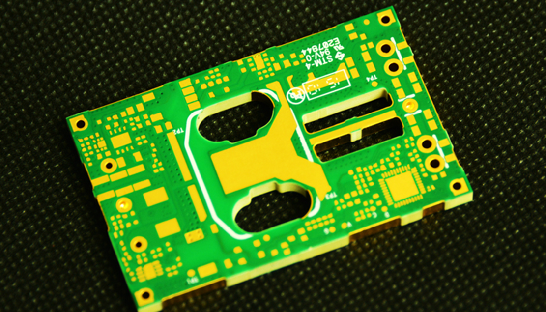
Heavy Copper Circuit Construction
Standard printed circuit boards, whether double-sided or multilayer, are manufactured
using a combination of copper etching and plating processes. Circuit layers start as
thin sheets of copper foil that are etched to remove unwanted copper, and plated to add
copper thickness to planes, traces, pads and plated-through-holes. All of the circuit
layers are laminated into a complete package using an epoxy-based substrate, such as FR4
or polyimide.
Boards incorporating heavy copper circuits are produced in exactly the same way, albeit
with specialized etching and plating techniques, such as high-speed/step plating and
differential etching. Historically, heavy copper features were formed entirely by
etching thick copper clad laminated board material, causing uneven trace sidewalls and
unacceptable undercutting. Advances in plating technology have allowed heavy copper
features to be formed with a combination of plating and etching, resulting in straight
sidewalls and negligible undercut.
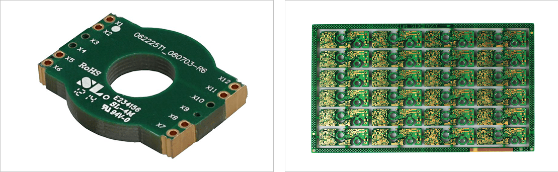
Plating of a heavy copper circuit enables the board fabricator to increase the amount of
copper thickness in plated holes and via sidewalls. It’s now possible to mix heavy
copper with standard features on a single board, also known as PowerLink. Advantages
include reduced layer count, low impedance power distribution, smaller footprints and
potential cost savings. Normally, high-current/high-power circuits and their control
circuits were produced separately on separate boards. Heavy copper plating makes it
possible to integrate high-current circuits and control circuits to realize a highly
dense yet simple board structure.
The heavy copper features can be seamlessly connected to standard circuits. Heavy copper
and standard features can be placed with minimal restriction provided the designer and
fabricator discuss manufacturing tolerances and abilities prior to final design


 Quote
Quote