


+86 13603063656
Modern electronic devices continue to shrink, accelerate, and integrate more advanced functions into smaller physical footprints. These rapidly tightening design envelopes force PCB engineers to rethink the way interconnects are created, how stacked structures behave under electrical stress, and how robust a board can remain while being assembled at high temperatures and intensities. In this context, Via-in-Pad technology has become one of the defining engineering features of high-density, high-performance electronics.
The technique represents a shift away from traditional via-to-pad separation and instead places the via structure directly beneath the component pad itself. On the surface, the concept seems elegantly simple: reduce routing distance and free up space. But underneath the solder, quite literally, lies a complex set of engineering constraints. These constraints span drilling tolerances, copper plating consistency, resin plug volume control, the planarity of filled and capped surfaces, solder wetting mechanics, assembly defect risk, and high-frequency electrical behavior.

Via-in-Pad
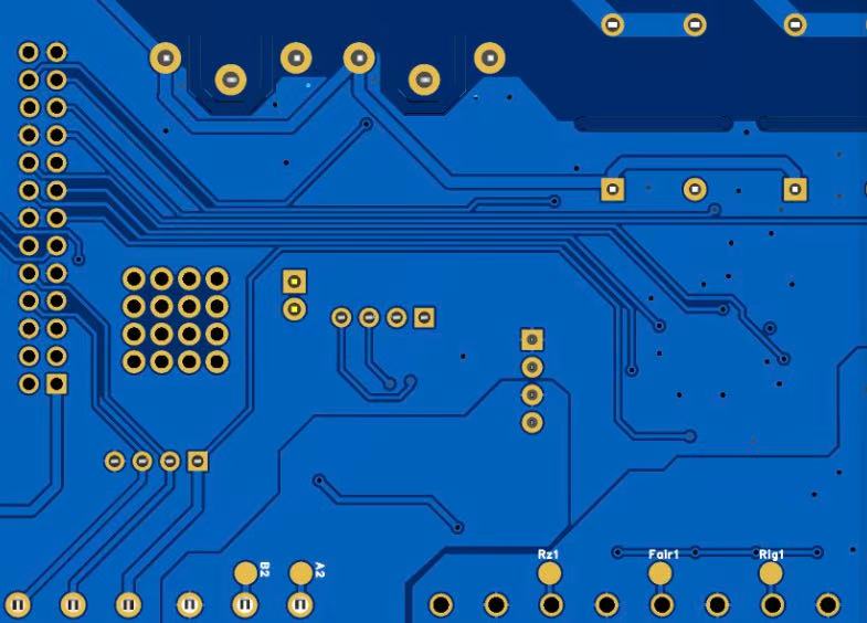
A Via-in-Pad feature is a via drilled directly into the component mounting pad—typically a BGA, LGA, QFN, or RF component pad—rather than being placed adjacent to it. This redesign changes the relationship between the pad and its associated interconnect, eliminating the small trace stub that traditionally connects the pad to a nearby via. In its simplest description, this structure consolidates the pad and via into one unified conductive and structural element that must satisfy both pad requirements and interconnect requirements simultaneously.
The fundamental elements of a Via-in-Pad structure include:
A drilled hole (either mechanically drilled or laser-drilled if microvia) located at the center or controlled-offset position of the pad.
Copper plating applied to the internal via walls to establish a conductive path.
Internal filling material, typically epoxy resin or copper paste, used to stabilize the hole.
A copper cap or planarization layer, which forms the final solderable pad surface.
These elements interact directly with solder, heat cycles, mechanical forces, and high-frequency currents, meaning that any variation in process quality can create problems that radiate up to assembly reliability and signal integrity.
The motivation for the structure is linked closely to device miniaturization and the restriction of escape routing space. Traditional designs use dog-bone fan-out patterns, but these consume routing room and impose layer count limitations. The Via-in-Pad structure breaks these constraints, particularly in packages with tight ball pitch such as 0.5 mm, 0.4 mm, or even 0.35 mm BGAs.
Because the via sits directly under the solderable pad, certain engineering conditions must be met:
The via must be fully sealed to prevent solder wicking.
The pad must remain planar for proper solder joint formation.
The copper cap must sustain the thermal cycles of reflow.
The filled via must hold structural integrity when subjected to assembly pressure.
Achieving these conditions requires precise control of both materials and production parameters—topics we will explore in depth throughout the remainder of this article.
Although the Via-in-Pad structure uses the same general terminology as other via types, it differs fundamentally in purpose, geometry, and constraints.
Traditional through-hole vias are positioned outside of the pad and are primarily designed for interlayer conduction. Their geometry is allowed to exhibit some level of barrel and annular ring variation, and they are not part of the soldering interface. They do not have to withstand the planarization, filling, or solder-bearing stresses that pad-integrated vias experience.
Microvias, while often used in HDI designs, are drilled into copper pads only when they form the top conductor layer in a stacked microvia structure. However, microvias used strictly for layer-to-layer transitions differ from Via-in-Pad structures because they are not simultaneously acting as solderable component pads. Via-in-Pad structures unify two roles—component mounting and via interconnection—that traditionally remain separate.
Additionally:
Microvias typically use laser drilling; Via-in-Pad structures may use laser or mechanical drilling depending on thickness.
Microvias are often placed on HDI interconnect layers; Via-in-Pad structures appear primarily under BGA or RF pad locations.
Microvias are rarely capped with copper for solderability; Via-in-Pad structures require this copper cap for a planar solder surface.
Understanding these differences is important because they shape the engineering rules and process controls manufacturers must implement.
The first major application category involves high-density components where traditional dog-bone escape routing becomes unfeasible. Ball grid arrays with sub-0.5 mm pitch, fine-pitch QFNs, and wafer-level chip scale packages benefit significantly from Via-in-Pad because the technique enables signal breakout within physically impossible constraints.
In many modern smartphones, tablets, VR systems, smartwatches, routers, and automotive ADAS modules, the Via-in-Pad strategy is the only viable path for routing signals from the IC’s central region. Without it, designers would be forced to increase the number of layers or compromise performance due to larger trace lengths.
High-frequency RF designs also rely heavily on Via-in-Pad to reduce parasitic inductance. Because the via sits directly beneath the signal source, the current path length is minimized, reducing high-frequency phase shift and improving return path stability.
A second major application category is power delivery networks in high-performance computing or data center hardware. Large BGAs used in server CPUs, FPGAs, and AI accelerators require low-impedance power paths. Via-in-Pad structures allow dedicated power vias to sit directly beneath the power pad, distributing current more uniformly into inner power planes.
This form of current distribution becomes essential at high switching speeds, such as VRM-driven CPU loads, where even small amounts of parasitic inductance can produce voltage drop spikes.
For designers seeking stable, manufacturing-robust Via-in-Pad implementation—especially in multi-laminate HDI or complex BGA footprints—JM PCB is a valuable partner due to their consistency in copper filling and pad planarity.
Via-in-Pad structures influence a PCB’s behavior in numerous ways:
Reduced inductance path: The direct vertical connection significantly minimizes inductive parasitics, improving high-frequency signal quality.
Less routing delay: Reduced routing length ensures shorter signal paths, which is especially important in DDR, PCIe, SerDes, and RF modules.
Enhanced return path control: Vias placed directly beneath the pad create efficient vertical return paths for differential signals.
Improved pad stability when properly filled: A filled and capped via behaves like a solid pad, distributing mechanical load.
Potential risk of pad sinking: If filling is incomplete, thermal expansion can cause microscopic sinking of the pad surface, affecting solder joints.
Enhanced heat transfer to inner layers: The via acts as a thermal conduit.
Risk of thermal cracking if filling materials have mismatched expansion coefficients.
Each of these performance influences introduces engineering challenges that must be controlled using careful process selection, precise drill and fill techniques, and compatibility testing between resin, copper, and laminate materials.
Later in the article, we will discuss how these constraints intersect with manufacturability.
Via-in-Pad should not always be used by default. It is an engineering-driven decision based on trade-offs among density, reliability, cost, and assembly complexity.
Situations where Via-in-Pad is ideal include:
Extremely tight BGA fan-out requirements.
High-frequency RF functions requiring reduced inductance.
Power rails needing short, direct vertical conduction.
Designs where layer count must be minimized.
Cases where routing channels are severely restricted by mechanical constraints.
Situations where Via-in-Pad may not be ideal include:
Low-cost consumer boards with no routing constraints.
Designs where via filling and planarization add unnecessary cost.
Boards where thermal stress is high and resin stability is questionable.
Solder-heavy applications where cap quality must be exceptionally consistent.
Engineers should consider the entire design ecosystem, from PCB stackup to component reliability expectations.
When engineers discuss Via-in-Pad structures, it is tempting to focus only on the advantage of saving routing space. However, the true complexity is hidden inside the via cavity and below the copper cap, where multiple materials must coexist in perfect dimensional and thermal harmony. This internal configuration demands manufacturing precision that exceeds the requirements of traditional via structures.
The principal engineering challenge arises from the need to transform a hollow drilled via into a mechanically solid, planar, and solderable surface—one that behaves as though the via never existed at all. This is achieved only when the via is filled with an appropriate resin or copper material, cured, planarized, and then plated with a controlled copper thickness that allows reliable solder joint formation.
A Via-in-Pad feature introduces all of the following manufacturing requirements simultaneously:
Ultra-precise drilling tolerance
The via must be placed at the exact center of the component pad, and its walls must be smooth enough to ensure reliable plating. Deviations in drilling tolerance directly affect filling uniformity and finished pad planarity.
Consistent copper plating thickness
Barrel plating must remain uniform. Variations can change via resistance, stress distribution, and thermal expansion behavior.
Void-free via filling
Any void inside the filled cavity—even microscopic ones—can cause expansion, cracking, or pad sinking during reflow.
Planarization accuracy
After filling, the via must be sanded or polished to ensure surface flatness before copper capping. Uneven planarization can cause solder imbalance, component tilt, or open circuits.
Copper capping reliability
The final copper cap must remain structurally stable during thermal cycles within the assembly process.
These requirements must be fulfilled within tight tolerances, especially when designing for BGA packages with pitches below 0.5 mm. Even a 5–10 μm deviation from planarity can affect solder performance.
Drilling a hollow structure directly beneath a component pad leaves no margin for placement errors. Traditional via placement allows small positional variations because the via is offset from the pad. In Via-in-Pad, this tolerance is removed, meaning that positional errors translate directly into pad misalignment.
When mechanical drilling is used:
Bit wander must be minimized to below 10–20 μm.
Drill bits must be replaced frequently to maintain bore smoothness.
Hit-count control must prevent degradation of bit edge quality.
Entry and backup materials must be matched carefully to laminate hardness.
Drill smear also becomes a larger concern because smearing on via walls reduces adhesion between copper plating and substrate, which can introduce barrel cracking during assembly.
Laser drilling is used for microvias typically 75–125 μm in diameter. When a Via-in-Pad structure requires microvia-sized holes, engineers must control:
CO₂ or UV laser pulse energy
Focus depth to avoid over-burning into adjacent layers
Laser aperture to prevent irregular hole diameters
Debris removal to maintain plating adhesion
The drill shape must be consistent across hundreds or thousands of holes, especially in multi-laminate HDI structures.
A Via-in-Pad structure may look mechanically simple—a filled via under a pad—but its reliability is influenced by an interconnected set of stress factors. These factors include thermal cycling from reflow soldering, mechanical strain from component mounting, differential expansion between resin and copper, and electrical behavior at high frequencies.
During reflow soldering, the PCB experiences multiple rapid temperature transitions. A typical lead-free reflow profile may reach 245–255°C at peak. Within a Via-in-Pad structure, different materials experience thermal expansion at different rates:
Copper plating
Epoxy resin fill
Substrate dielectric
Copper cap
Solder alloy
Because these materials expand differently, internal stress accumulates. If the resin expands faster than the copper barrel, micro-cracks may develop at the interface, especially at the knee (transition between pad and via wall). If copper expands faster, resin cracking may occur.
Thermal reliability depends heavily on:
Resin CTE (Coefficient of Thermal Expansion)
Resin curing process and shrinkage behavior
Copper plating thickness uniformity
Smoothness of via wall after desmear
Structural symmetry around the pad
When thermal mismatch becomes excessive, the failure modes include:
Barrel cracking
Cap-pad shear cracking
Solder joint voids
Component tilt under BGA
Microfractures detectable only under cross-section analysis
This is why material choice—especially the resin formulation—is one of the most critical engineering decisions when implementing Via-in-Pad.
Mechanical stress in Via-in-Pad occurs primarily during:
SMT pick-and-place mounting
Solder joint solidification
Board flexing during assembly or final use
Thermal warpage of large BGAs
The filled via behaves like a pillar beneath the pad. If the fill material is weak or uneven, the pad may deform under pressure. Excessive flex could cause:
Resin cracking
Deformation of the copper cap
Pad lifting
Internal delamination
Mechanical reliability is especially critical in large BGA packages such as CPU, GPU, FPGA, and networking ASIC footprints.
Via-in-Pad improves electrical performance by reducing inductance and return path length. However, poor filling or plating can weaken electrical consistency.
Risk factors include:
Voids inside the fill, altering current density
Thin plating, increasing via resistance
Barrel thickness asymmetry, causing uneven current distribution
Copper cap voids, affecting RF surface conductivity
At high frequencies (GHz range), even very small geometric inconsistencies can affect signal quality.
Via-in-Pad failures typically do not appear visually. They must be detected using:
Used to reveal:
Solder voids
Solder wicking into poorly sealed vias
Pad tilt or ball irregularity
Internal gaps beneath BGA balls
A cross-section reveals:
Internal voids inside fill material
Copper barrel cracks
Resin cracking
Curling or delamination beneath the copper cap
A stress test for BGA reliability. Dye penetrates cracks; prying reveals where dye spreads.
Detects delamination and voids beneath pad surfaces.
For high-speed designs, Time-Domain Reflectometry verifies impedance discontinuities caused by via inconsistencies.
These detection methods allow engineers to refine process parameters and improve reliability.
| Parameter | Conventional Via | Via-in-Pad | Engineering Insight |
|---|---|---|---|
| Placement Location | Next to the pad | Inside the pad | Via-in-Pad improves routing density but raises process complexity |
| PCB Density | Moderate | Very high | Ideal for HDI and fine-pitch packages |
| Thermal Path | Longer | Direct and shorter | Enhances heat extraction in power devices |
| Signal Integrity | Possible parasitic inductance | Lower parasitics | Beneficial for RF/high-speed interfaces |
| Solderability Risk | Low | Higher without proper filling | Requires resin plugging + planarization |
| Ideal Use Cases | Standard multilayers | HDI, BGA, CSP, micro-pitch ICs | Advanced packaging advantage |
Via-in-Pad structures embody the hidden sophistication of today’s PCB manufacturing. They compress mechanical, electrical, thermal, and material disciplines into a single integrated feature buried beneath the solder pad. Success depends on:
Tight drilling tolerances
High-quality resin or copper filling
Meticulous planarization
Controlled copper capping
Advanced HDI stackups
Qualified manufacturing partners
While Via-in-Pad dramatically enhances routing density, signal integrity, and thermal dissipation, it also introduces one of the most demanding engineering challenges in modern PCB fabrication.
In the era of miniaturization and high-frequency design, Via-in-Pad is not just an option—it is a necessity. But mastering it requires engineering precision at every buried layer beneath the solder.
Via-in-Pad is a PCB structure in which a via is drilled directly inside a component pad. The via is filled, cured, planarized, and capped with copper so the pad remains solderable.
It enables space-efficient breakout routing, reduces via inductance, shortens signal paths, and improves electrical and thermal performance.
Yes. Via-in-Pad shortens vertical transitions, reduces parasitic inductance, and supports better impedance continuity for GHz-range signals.
Common fill materials include copper paste and epoxy resin. Each has different thermal, mechanical, and cost characteristics.
Potential failures include resin voids, copper cap cracking, barrel fractures, solder wicking, pad tilt, and internal delamination.


Connect to a Jerico Multilayer PCB engineer to support your project!
Request A Quote


 Quote
Quote