


+86 13603063656
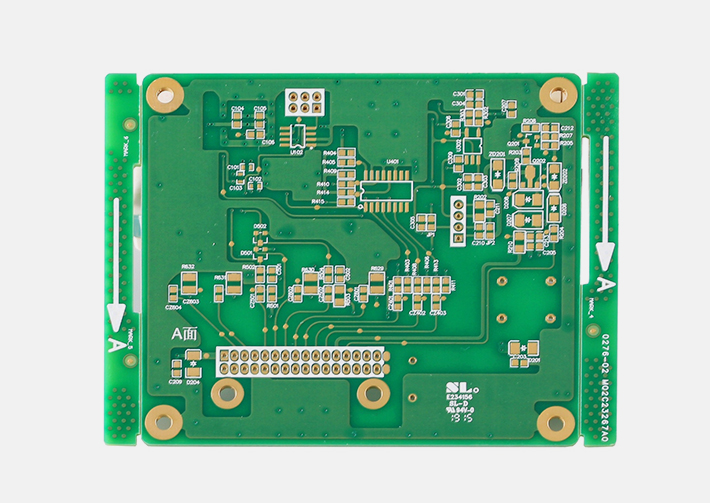
One-stop PCBA wise manufacturers today to tell you what causes BGA soldering bad problems?PCB design of several common problems. In PCBA processing, due to improper PCB design, often encounter the problem of poor BGA welding. Next Leadjo PCBA on bad BGA welding PCB design of several common problems summarized analysis.
Incorrect PCB design leads to the analysis of BGA welding defects
1. The hole at the bottom of the BGA has not been processed
BGA welding board with holes, the ball will be lost with the solder during the welding process; due to the lack of resistance welding process in PCB production, solder and solder balls will be lost through the holes close to the board, resulting in the loss of solder balls, as shown in the figure below.
2. Poor design of BGA resistance solder film
PCB solder loss will be caused by through holes in the solder pad; in high density assembly, micro-hole, blind hole or plug hole processes must be used to prevent solder loss; as shown in the figure below, wave soldering is used and there are holes at the bottom of the BGA. After wave soldering, the solder on the holes can affect the reliability of the BGA soldering, which can lead to defects, such as short circuiting of the assembly.
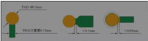
3. BGA solder board design
The exit line of BGA solder plate should not exceed 50% of the diameter of the solder plate, and the exit line of power solder plate should be not less than 0.1mm, and then it can be thickened. To prevent the deformation of the welding plate, the welding blocking window should not be larger than 0.05mm, as shown in the figure below.
4. The size of the solder board is not standard, too big or too small, as shown in the following figure.
5. The size of BGA pads are different and the solder joints are irregularly rounded with different size circles as shown below.
6. The distance between the outer frame of the BGA and the edge of the body of the component is too small
All parts of the component should be located within the marking line. The distance between the frame line and the package edge of the component should be greater than 1/2 the size of the solder end of the component, as shown in the figure


Connect to a Jerico Multilayer PCB engineer to support your project!
Request A Quote


 Quote
Quote