


+86 13603063656
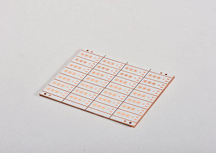
A copper clad PCB is a type of PCB that features a copper clad laminate. This laminate is a PCB substrate that plays a significant role in PCB manufacturing. A copper clad board is common in the PCB industry. This is because it offers great features. It is an ideal option for high-frequency applications.
Copper clad laminates are widely used to design copper clad boards. These laminates soak in resin with some reinforcing material to make copper clad boards. Copper clad PCBs are available in computers, television, and other electronic devices.
The importance of copper clad is to enhance anti-jamming capability and minimize ground wire’s impedance. Copper clad also reduces the voltage drop of a circuit board. The copper clad boards feature glass fiber as a reinforcing material.
Copper PCB board is lightweight, strong, and durable. This board features electromagnetic shielding benefits. Several industries, including the military, incorporate this board in their devices.
Features of the Best Copper Clad PCB
You know the best copper clad PCB board through the feature it possesses. The following features are what make good-quality copper clad boards;
Exceptional chemical performance
It is important to note the chemical performance of a copper clad PCB. A copper clad board with great chemical performance is ideal for electronic devices. The chemical performance of this PCB must meet the stringent requirements for Tg. Also, it must meet the requirements for CTE on a Z-axis and chemical regents resistance.
Great Appearance
The appearance of a copper clad board matters a lot. There are issues that could happen due to unforeseen elements in the fabrication process. Issues like resin points, scratches, wrinkles, and more could occur. If a copper clad board has any of these issues, it will cause poor performance.
Exceptional Physical performance
The physical performance of a copper clad laminate includes peel strength. A copper clad must also feature great heat resistance and dimensional stability. These are some of the attributes that make up the best copper clad PCB.
Size
A copper clad PCB features a copper clad laminate as the base material. Therefore, this laminate must meet some size requirements as regards the intended end design. Manufacturers must consider all parameters. These include the diagonal deviation, length, and width. Meeting these requirements birth an effective copper clad PCB.
Good electrical performance
The best copper clad laminate features a good electrical performance. Manufacturers need to meet strict requirements like dissipation factor and volume resistance.
Why is Copper Used in PCB?
double sided copper clad boarddouble sided copper clad board
Copper is one of the most common materials used in PCB manufacturing. The most significant and popular benefit of copper is its high conductivity. Copper is a highly conductive material that can transmit signals easily. It doesn’t lose electricity while transmitting these signals.
PCB manufacturers don’t need to use tons of copper during manufacturing. A small amount of copper has a significant impact. An ounce of copper can cover a whole square foot of a circuit board substrate. Another benefit of copper is that it is widely available and inexpensive. It is a cheaper alternative to other materials.
Circuit boards need electricity to function well. The titular circuits in PCBs are crucial pathways that distribute electric charges from one place to another. These pathways must carry the charges efficiently. Although other materials can carry these electric charges, copper is conductive. Therefore, it is a standard option in the rigid flex PCB industry.
Copper is highly conductive because it features one valence electron. Such electrons can move from one atom to another without much resistance. Electrons are basic particles that carry electrical charges. Therefore, valence electrons transfer electrical signals. With all these features, copper is considered the ideal element for cladding PCBs.
What is a Double Sided Copper Clad Board?
Copper Clad boards are available in single sided and double sided. A double sided copper clad PCB features two sided copper traces with a bottom and top layer. These boards feature conductive copper on the two sides of the circuit board.
Double sided copper clad boards are one of the most common PCBs. These boards allow manufacturers to design complex circuits. Double sided copper clad boards are ideal in higher technology applications. Vending machines, lighting systems, and more feature double sided copper clad boards.
Manufacturers prefer double sided copper boards because they use more complex circuitry. The greatest advantage of these boards is that there is an extra layer where you can add more components. This helps to increase the circuit’s density.
Where are copper clad boards used?
Copper clad boards are ideal for use in several applications. You will find these boards in consumer electronics like computers, television, and radio. They are also widely used in applications that require high frequency. These boards are ideal for use in the telecommunication industry.
What are the standards for copper clad PCBs?
According to ASTM D1867, copper boards must meet peel strength at high temperatures. These boards must also feature lengthwise and crosswise flexural strength. Copper clad boards must also conform to tests for twist, warp, and blistering. Copper clad PCB manufacturers have to follow the IPC-4101C standard. The IPC-IM 650 is the standard test for copper clad boards.


Connect to a Jerico Multilayer PCB engineer to support your project!
Request A Quote


 Quote
Quote