


+86 13603063656
Printed Circuit Boards (PCBs) are the skeletal framework of nearly all modern electronics. Among the many process steps and quality checks a PCB must undergo, the ability of the copper pads to accept solder — often referred to as “tinning” or “solderability” — remains a decisive indicator of quality. When pads fail to take solder properly, yields decrease, rework increases, and reliability is compromised. This article, “From Oxidation to Contamination: A Comprehensive Analysis of What Makes PCB Pads Difficult to Tin,” provides an in-depth examination of why this problem arises, what materials and processes are at play, and how engineers and manufacturers can prevent it.
A comprehensive understanding of the underlying causes begins with a look at materials, surface chemistry, and process control. Each section of this article delves deeply into a specific factor, building a picture of the interconnected nature of PCB manufacturing. It also introduces real-world practices such as better surface preparation, modern protective finishes, and strict quality control.
In addition, this analysis highlights the importance of selecting experienced and technologically advanced partners. By exploring the interplay between material science and production technology, this article equips PCB designers, process engineers, and purchasing managers with a practical roadmap to improved solderability and better yields.

What Makes PCB Pads Difficult to Tin
The first step in solving any manufacturing problem is to define it clearly. What Makes PCB Pads Difficult to Tin is not a single defect but rather a cluster of related phenomena. Pads may appear shiny and conductive yet still resist solder, or they may display visible discoloration or residues. Common symptoms include poor solder wetting, non-wetting areas, partial solder fillets, and outright solder beading off the pad surface. These issues undermine both automated and manual soldering operations.
Tinning is the process of coating copper pads with a layer of solder, either during PCB fabrication or during the assembly process. This layer improves solderability, protects against oxidation, and ensures reliable electrical and mechanical connections between the PCB and components. When What Makes PCB Pads Difficult to Tin arises, solder fails to wet or adhere properly, leading to increased joint resistance, potential intermittent connections, and reduced lifetime.
Earlier PCB manufacturing methods relied heavily on simple tin-lead plating, which provided an inherent barrier against oxidation. However, with environmental regulations and the advent of lead-free soldering, alternative surface finishes have proliferated: OSP (Organic Solderability Preservatives), immersion tin, immersion silver, ENIG (Electroless Nickel Immersion Gold), and more. Each finish has distinct advantages and trade-offs, but all must contend with the same fundamental issue: copper’s natural tendency to oxidize and accumulate contaminants.
This diversification of finishes has, paradoxically, made What Makes PCB Pads Difficult to Tin a more complex topic. It’s no longer just about copper oxide layers; it’s about how each finish interacts with flux chemistry, reflow profiles, storage conditions, and handling practices.
At the microscopic level, copper is highly reactive. Even trace oxygen and moisture can form oxides within hours. Add to this the presence of halides, organic residues, or improper rinsing during fabrication, and you have a surface that no longer behaves as pristine metal. In the context of What Makes PCB Pads Difficult to Tin, such changes at the atomic scale translate into macroscopic defects during soldering.
The solder joint is not just a mechanical bond but also a key part of the circuit’s electrical path. High contact resistance due to incomplete wetting can result in voltage drops, signal integrity issues, or heat buildup. For high-frequency and high-power applications, these problems can be catastrophic. Thus, avoiding What Makes PCB Pads Difficult to Tin is not merely about cosmetic quality; it’s about ensuring the long-term reliability and performance of the product.
Addressing What Makes PCB Pads Difficult to Tin often requires collaboration across the supply chain. PCB fabricators, assembly houses, and materials suppliers must share process data, conduct joint root-cause analyses, and standardize cleaning and handling procedures.
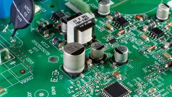
Material selection is one of the earliest and most influential decisions in PCB manufacturing. The choice of copper foil type, laminate properties, and surface finish directly determines how easily solder will wet the pads. In other words, before soldering even begins, your material stack-up can predetermine What Makes PCB Pads Difficult to Tin.
Copper foils come in two dominant forms — rolled (RA) and electrolytic (ED). Each has distinct microstructures and surface textures. Rolled copper foil is produced by mechanically rolling a thick copper sheet to the desired thickness. Electrolytic copper foil, by contrast, is grown in a plating bath on a rotating drum, then peeled off. The resulting grain structure, surface roughness, and mechanical properties all influence how well the copper can be finished and later soldered.
Rolled copper foils usually offer smoother surfaces and fewer nodules, which can make flux and solder flow more uniformly. Electrolytic foils tend to have more pronounced surface profiles, which can improve mechanical adhesion to the dielectric but also present more area for oxidation or contamination. Understanding this difference is crucial when considering What Makes PCB Pads Difficult to Tin at the manufacturing stage.
The resin content, glass weave, and coefficient of thermal expansion (CTE) of the laminate may seem unrelated to solderability. However, these factors determine how stable the copper adhesion remains through multiple thermal cycles. If micro-delamination or pad lifting occurs, flux can be trapped, and localized oxidation may worsen. Therefore, the substrate and copper must be matched carefully to ensure robust performance and prevent What Makes PCB Pads Difficult to Tin.
The selection of a surface finish — ENIG, immersion silver, immersion tin, OSP — directly influences solderability. For example, OSP is highly dependent on handling conditions; even fingerprints can disrupt the organic layer and cause localized non-wetting. ENIG offers a durable barrier but can develop black pad issues if the nickel layer is compromised. Each finish has its own optimal shelf life and storage requirements. By choosing the right finish for the intended environment and assembly process, you can minimize What Makes PCB Pads Difficult to Tin.
Even the smoothest copper foil needs to be cleaned and activated before plating or applying a finish. This involves micro-etching, rinsing, and sometimes plasma treatment to remove residues. Skipping or shortening these steps risks leaving organics or oxides on the surface, which later manifest as What Makes PCB Pads Difficult to Tin during assembly.
Select appropriate copper foil: If your application demands extremely fine-pitch soldering or high reliability, consider rolled copper foil for smoother surfaces.
Use finishes suited to your environment: High-humidity storage might favor ENIG or immersion tin over OSP.
Insist on supplier cleanliness: Work with fabricators who can provide objective cleanliness and solderability data.
While premium materials and finishes can cost more upfront, they often yield significant savings by reducing rework, field failures, and warranty returns. The cost of a single assembly defect, especially in high-value electronics, can dwarf the incremental cost of higher-quality materials. Thus, thinking strategically about your material selection directly mitigates What Makes PCB Pads Difficult to Tin and improves total cost of ownership.
If there is one dominant and universal cause of poor solderability, it is the formation of oxides and corrosion products on the copper surface. Copper, nickel, and even precious metals like gold will tarnish over time if conditions are unfavorable. Understanding the mechanisms of oxidation and corrosion is essential for preventing What Makes PCB Pads Difficult to Tin at the assembly stage.
Copper reacts readily with oxygen and moisture in the air. The moment copper surfaces emerge from an etching bath or are exposed after drilling, a thin oxide layer begins to form. Initially only a few atoms thick, this layer can grow thicker and more complex if the board is exposed to humidity, acids, or handling residues. Even fingerprints contain chloride ions that accelerate corrosion.
From the standpoint of solderability, this oxide layer acts like an insulator. Fluxes designed for lead-free solders have limited activity compared to older tin-lead fluxes, which means they are less capable of breaking down heavy oxides. This interplay between modern flux chemistry and oxidation is a major factor in What Makes PCB Pads Difficult to Tin.
Many PCB pads are not pure copper but consist of copper plated with nickel and then covered by a thin layer of gold (ENIG) or other finishes. These mixed-metal systems can develop galvanic corrosion if the layers are poorly deposited or contaminated. For instance, “black pad” is a well-known defect in ENIG finishes where the nickel becomes corroded, leading to non-wetting during soldering. Such defects directly manifest as What Makes PCB Pads Difficult to Tin at the reflow stage.
Humidity and Temperature: Higher moisture content in storage areas speeds up oxidation.
Pollutants: Sulfur compounds from industrial environments or packaging materials can tarnish copper quickly.
Storage Duration: The longer a PCB sits between fabrication and assembly, the thicker the oxide layer becomes.
This is why IPC and other standards specify shelf lives for various finishes. Exceeding these windows without proper re-treatment nearly guarantees What Makes PCB Pads Difficult to Tin.
Controlled Atmosphere Storage: Using nitrogen cabinets or desiccant packs to reduce moisture and oxygen exposure.
Timely Assembly: Shorten the time between board fabrication and soldering to minimize oxidation buildup.
Protective Coatings: Apply OSP or conformal coatings as temporary barriers until assembly.
Pre-Solder Cleaning: Employ micro-etching, plasma cleaning, or chemical activation just before soldering to restore the pristine copper surface.
Even the best surface finish cannot survive improper handling. Operators should wear gloves, avoid touching pads directly, and use clean trays. Packaging materials should be free of sulfur and other reactive chemicals. Every extra precaution reduces the risk of What Makes PCB Pads Difficult to Tin.
Track Finish Age: Maintain a database of board lot numbers, finish type, and expiration dates to ensure boards are assembled within their solderability window.
Audit Storage Conditions: Periodically check humidity, temperature, and cleanliness of storage areas.
Work with Responsive Suppliers: Suppliers such as JM PCB provide documentation and inspection reports that help customers know exactly when to assemble their boards for best solderability.
If oxidation is not addressed, the result is increased soldering time, higher flux usage, greater rework, and potential field failures. All of these increase total cost. Taking proactive steps against oxidation — at both the fabricator and assembler level — eliminates a major source of What Makes PCB Pads Difficult to Tin.
Beyond oxidation, contamination is the second most common reason why solder refuses to wet a PCB pad. Contaminants range from invisible ionic residues to obvious particles or films left over from the fabrication process. Understanding where contamination comes from and how to control it is vital to reducing What Makes PCB Pads Difficult to Tin.
Etching and Plating Residues: Incomplete rinsing after chemical processes can leave salts or acids on the surface.
Photoresist Residues: Traces of dry film or liquid photoresist may remain if stripping is incomplete.
Debris from Drilling or Routing: Fiberglass particles or drill smear can settle onto pads.
Flux and Solder Mask Bleed: Poorly cured solder mask or misapplied flux can create thin films.
Each of these contaminants interferes with flux activity and solder wetting, contributing directly to What Makes PCB Pads Difficult to Tin.
Ionic residues, such as chlorides or sulfates, are particularly harmful because they can form conductive paths or accelerate corrosion. Non-ionic contaminants, like oils and greases, primarily act as physical barriers. Both types reduce solderability but may require different cleaning methods. For example, ionic contamination is often measured by Ion Chromatography (IC) or Resistivity of Solvent Extract (ROSE) testing to quantify its presence.
Modern lead-free fluxes have lower activity levels to comply with environmental standards. While this reduces harmful residues, it also means they’re less effective at breaking down heavy contamination. If the PCB pads are dirty, even the best flux cannot fully restore wetting. Thus, contamination control upstream is the best defense against What Makes PCB Pads Difficult to Tin.
Introducing a cleanroom or at least controlled environments for key steps can dramatically reduce contamination. Key measures include:
Air filtration to reduce particulate matter
Antistatic mats and ionizers to prevent particle attraction
Gloves and gowns to minimize operator contamination
Dedicated storage trays and covers for PCBs
Such practices mirror those used in semiconductor packaging, and they directly translate to fewer cases of What Makes PCB Pads Difficult to Tin.
Aqueous Cleaning: Uses deionized water and saponifiers to remove ionic and organic residues.
Solvent Cleaning: Effective for non-ionic residues like oils.
Plasma Cleaning: Removes thin organic films and activates the surface for soldering.
Combining these cleaning steps just before assembly can restore a pristine pad surface and prevent What Makes PCB Pads Difficult to Tin.
Strong coordination between design, fabrication, and assembly partners is crucial. For example:
Specify maximum allowable ionic contamination in purchase orders.
Require documentation of cleaning steps from your PCB supplier.
Schedule periodic audits to verify adherence to cleanliness standards.
JM PCB, for instance, integrates advanced rinsing systems and in-line cleanliness testing. These investments allow them to guarantee boards arrive with minimal contamination, reducing the risk of What Makes PCB Pads Difficult to Tin.
Even minor contamination can result in localized non-wetting, solder bridges, or latent corrosion. These defects often escape initial testing and manifest as field failures, which are far costlier than prevention. By proactively managing contamination, manufacturers significantly cut down on rework and improve long-term reliability.
Even when oxidation and contamination are under control, the microscopic topography of a PCB pad can still inhibit solder wetting. Surface roughness and underlying microstructure play a subtle but decisive role in What Makes PCB Pads Difficult to Tin.
Copper foil is composed of grains whose size and orientation affect how solder interacts with the surface. Rolled copper foil tends to have elongated grains and smoother surfaces, while electrolytic foil exhibits more nodular profiles. A smoother surface generally improves solder wetting because flux can more easily cover and activate it. Conversely, an overly rough or uneven surface traps flux residues, micro-particles, and air pockets, creating localized areas of non-wetting that add up to What Makes PCB Pads Difficult to Tin.
Many PCB pads are plated with additional copper, nickel, or other metals to meet thickness or performance requirements. If this plating is uneven — too thin in some areas, too thick in others — solder may not flow uniformly. Irregular pad geometry can also disrupt the thermal profile during reflow, leading to cold spots where solder fails to wet. Each of these factors reinforces What Makes PCB Pads Difficult to Tin by introducing local inconsistencies.
Whether you’re using ENIG, immersion tin, or OSP, consistency of thickness matters. A thin or worn-out layer may expose copper prematurely, while an excessively thick layer may crack or peel. Both conditions interfere with wetting. Periodic cross-section analysis and X-ray fluorescence (XRF) measurements can verify that finishes meet specifications and prevent What Makes PCB Pads Difficult to Tin.
Mechanical or chemical polishing just before assembly can remove minor oxides and smooth the surface. Common approaches include:
Micro-etching: A mild chemical treatment to clean and roughen slightly for improved solder adhesion.
Brushing or pumice scrubbing: Removes surface films and provides uniform texture.
Plasma cleaning: Improves wettability and removes organic contamination at a molecular level.
When properly controlled, these steps restore solderability without over-roughening the surface. This balance is critical to avoiding What Makes PCB Pads Difficult to Tin.
Pad size, spacing, and solder mask clearance all interact with surface roughness. For example, solder mask-defined pads can have slightly raised edges or trapped flux, while non-solder mask-defined pads might offer a cleaner surface for solder wetting. Designers should consider these factors early, as layout decisions directly affect assembly yield and can either mitigate or exacerbate What Makes PCB Pads Difficult to Tin.
Specify surface roughness targets: Work with suppliers who can measure and report Ra (average roughness) values.
Ensure consistent plating processes: Use automated lines and statistical process control to maintain uniform finishes.
Verify pad geometry in CAM review: Prevent inadvertent solder mask encroachment or uneven copper deposition.
Investing in tighter microstructural control at the fabricator level can pay off handsomely in the assembly phase. Fewer soldering issues mean less rework, less scrap, and higher throughput. For high-volume or high-value applications, these gains can far exceed the incremental cost of improved surface quality.
No matter how carefully a PCB is designed and fabricated, it is impossible to be certain of its solderability without testing. Objective, repeatable testing allows engineers to detect potential issues long before they reach the assembly line. In this section we explore the main diagnostic techniques used to identify What Makes PCB Pads Difficult to Tin.
Solderability testing provides measurable data on how easily solder wets a pad under defined conditions. Without it, defects may only become visible during assembly, when rework is costly. Incorporating solderability testing into incoming inspection or in-process checks can dramatically reduce failures linked to What Makes PCB Pads Difficult to Tin.
Wetting Balance Test: Measures the force of molten solder wetting a pad over time. A low wetting force or delayed time indicates poor solderability.
Dip-and-Look Test: Involves dipping the test specimen into molten solder and then visually examining the coverage.
Surface Insulation Resistance (SIR) Testing: Evaluates contamination and ionic residues that can indirectly affect solderability.
X-Ray Fluorescence (XRF): Confirms finish thickness and composition, which directly influence wetting.
These methods, when used together, provide a comprehensive picture of What Makes PCB Pads Difficult to Tin.
High-magnification optical microscopes and scanning electron microscopes (SEM) can reveal micro-cracks, plating voids, or residues invisible to the naked eye. Energy Dispersive Spectroscopy (EDS) attached to SEM systems can identify chemical composition at specific sites. This allows pinpointing the root cause of What Makes PCB Pads Difficult to Tin at a granular level.
Ionic contamination testing is essential for evaluating the cleanliness of PCBs. By identifying the type and quantity of ionic residues, engineers can correlate them with solderability defects. When test results exceed acceptable thresholds, corrective action can be taken upstream to prevent What Makes PCB Pads Difficult to Tin.
Cutting a cross-section of a pad and inspecting it under a microscope reveals plating thickness, intermetallic layers, and the presence of voids or inclusions. This method is especially useful for diagnosing mixed-metal finishes like ENIG, where “black pad” or nickel corrosion can be root causes of What Makes PCB Pads Difficult to Tin.
Track Key Variables: Bath chemistry, temperature, pH, and agitation directly affect plating quality.
Set Control Limits: Monitor each parameter statistically to catch drifts before they cause defects.
Use Automated Data Collection: This ensures timely detection of trends leading to What Makes PCB Pads Difficult to Tin.
Once test data identifies a pattern, preventive measures can be implemented:
Adjust surface preparation or cleaning steps.
Modify storage conditions or shelf life policies.
Switch to a more robust finish.
Select a supplier with stronger quality controls, such as JM PCB, which employs in-line solderability testing to catch issues before shipment.
Early detection saves time, reduces rework, and minimizes the risk of field failures. For high-reliability products, solderability testing is not an option but a necessity. By identifying and mitigating What Makes PCB Pads Difficult to Tin at the earliest stages, companies reduce costs and improve customer satisfaction.
Addressing what makes PCB pads difficult to tin requires a holistic approach that spans materials, design, fabrication, assembly, and supplier collaboration. The recurring theme across all sections is that no single factor alone causes solderability issues—oxidation, contamination, surface microstructure, pad geometry, handling, and process control all interact to influence tinning performance.
Oxidation and Contamination Are Primary Factors
Surface oxidation and chemical contamination remain the most common causes of poor wetting. Proactive cleaning, surface activation, and proper storage are essential preventive measures.
Surface Microstructure Matters
Copper grain orientation, plating uniformity, and finish thickness directly affect solderability. Micro-etching, smooth finishes, and regular inspections improve wetting.
Process Control Reduces Variability
Statistical process control, inline inspection, and predictive maintenance minimize defects before they reach assembly. Consistent process parameters ensure reproducible tinning performance.
Supplier Selection and Coordination Are Critical
High-quality materials and finishes, combined with stringent supplier audits, reduce variability and contamination risk. Trusted suppliers like JM PCB provide robust quality control, traceability, and advanced surface treatments that directly address solderability challenges.
Assembly Practices Are the Final Determinant
Flux selection, solder paste type, thermal profiling, and handling protocols ensure that even high-quality boards achieve proper wetting. Ignoring assembly practices can negate upstream improvements.
Emerging Innovations Offer Future Improvements
Advanced surface finishes, plasma and laser treatments, AI-driven process monitoring, and eco-friendly materials all contribute to reducing what makes PCB pads difficult to tin in next-generation electronics.
Implement rigorous pre-assembly cleaning and surface activation procedures.
Select finishes appropriate for board type, storage conditions, and assembly method.
Monitor surface roughness, plating thickness, and chemical composition using XRF, SEM, or AOI tools.
Establish robust incoming material control and work with trusted suppliers, such as JM PCB, to ensure surface integrity.
Optimize solder paste, flux, and thermal profiles during assembly for consistent wetting.
Incorporate continuous training and handling protocols to minimize contamination from operators.
Explore new surface treatments and predictive monitoring technologies to preempt future tinning challenges.
Ultimately, preventing what makes PCB pads difficult to tin is about anticipating problems before they occur. Combining design foresight, controlled fabrication, careful material selection, and disciplined assembly practices ensures reliable solderability and high yield. The integration of emerging technologies and supplier collaboration positions manufacturers to meet the increasing demands of miniaturized, high-density, and lead-free electronics while maintaining robust performance and assembly efficiency.
What is the difference between rolled copper foil and electrolytic copper foil?
Rolled copper foil is mechanically rolled for smoother surfaces and higher mechanical strength. Electrolytic foil is deposited via electrolysis, is more flexible, and cost-effective.
How does OSP differ from immersion tin?
OSP uses a temporary organic layer to protect copper and is environmentally friendly but sensitive to handling. Immersion tin deposits a metallic layer directly on copper, offering stronger protection but requiring controlled storage.
Can solder paste selection improve wetting?
Yes, choosing flux with sufficient activity and a compatible solder paste can compensate for minor oxidation or contamination, enhancing wetting.
How does storage affect solderability?
Exposure to humidity, high temperature, or contaminants accelerates oxidation and degradation, causing poor tinning. Proper controlled storage extends shelf life and preserves wetting.
Can pad design influence solderability?
Absolutely. Pad size, spacing, and solder mask clearance affect wetting. Small, irregular, or masked pads can fail to wet fully, contributing to soldering challenges.


Connect to a Jerico Multilayer PCB engineer to support your project!
Request A Quote


 Quote
Quote