How to Make a PCB Board: Step-by-Step Guide for Professionals dives into every stage of PCB fabrication, from design to testing. This article walks B2B engineers, procurement managers, and R&D teams through the essential tools, materials, and techniques required to produce reliable PCBs in-house or via trusted suppliers. You’ll learn why each step matters, how to avoid common pitfalls, and when to scale up to professional manufacturing. By the end, you’ll understand how to efficiently create high-quality circuit boards and make informed choices that save time, reduce cost, and boost your product’s performance.
How to Make a PCB Board
So you want to make your own circuit board? But here’s the kicker… knowing how to make a PCB board isn’t just a DIY skill—it’s a strategic advantage. In today’s fast-paced electronics market, the ability to prototype, iterate, and validate designs in-house can reduce development cycles from weeks to days, giving companies a competitive edge in delivering tech solutions faster.
Ready for the good part? Let’s look at how smart organizations apply this capability. A midsize robotics firm used toner transfer PCB production to test control board revisions overnight—cutting its debugging cycle by 70%. A European medical device specialist leveraged homemade PCBs to qualify boards under real operating conditions before final production, ensuring compliance without expensive fab runs. Even automotive sensor developers are using mini PCB making to simulate electromagnetic behavior before tapping large fabs.
What’s the real story? Making a PCB isn’t just about circuit connectivity—it’s about capturing control over design iteration, reducing risk, and empowering agile engineering. But it’s critical to master the process chain: from layout to etching, drilling to finishing. Get it wrong, and you risk shorts, weak joints, or non-functional circuits.
| Benefit | Impact on Business | Example |
|---|---|---|
| Faster Iteration | Quicker prototyping cycles | Robotics firm cut debug time by 70% |
| Cost Control | Reduced reliance on external fab orders | Medical device prototype compliance |
| Design Flexibility | More design latitude and rapid changes | Automotive testing under EMI conditions |
With that solid foundation, we’ll explore each phase of PCB creation—starting now with the tools and materials you’ll need, how to design with intent, and how to execute every step with professional precision. Let’s dive in and learn how to make a PCB board the right way.
To make a PCB board you need more than just copper-clad board and acid—you need the right tools and materials. But here’s the kicker… quality in demands quality out. Equipping your lab with the right gear ensures reliability and professional results. Let’s unpack what you truly need.
First up, essential tools. A precision laser printer or copier is vital for toner transfer; an iron or laminator helps merge the toner to copper. You’ll need a rotary tool or drill press with carbide bits (0.3–1 mm) for component holes, and a small UV or LED curing station for solder mask application. Engineers often invest in a small fume hood for safe etching and ventilation. Don’t forget tweezers, countersink bits, multimeters, and anti-static wrist straps.
Next, materials make a dramatic difference. Copper-clad FR4 circuit boards come in single- and double-sided variants; choose quality with even copper thickness to avoid uneven etching. Toner cartridge, developer, and resist films ensure clean pattern transfer. For etching, ferric chloride is common, while ammonium persulfate offers cleaner, adjustable etch rates. A solder mask kit—UV photoresist plus developer—provides clean insulation and aesthetic appeal. High-quality rosin-core solder (63/37) and flux help prevent cold joints.
Here are three professional examples:
A European telecom startup sourced high-precision FR4 panels and used peristaltic pumps to circulate etching solution—improving uniformity. A medical device firm invested in a small drill press and bent shallow countersinks to reduce pad lift. An automotive test lab stocked each ion of conductive pen and solder resist to quickly fix layout adjustments on tight deadlines.
| Category | Item | Purpose |
|---|---|---|
| Design Output | Laser printer/copier | Deep toner density for accurate transfer |
| Substrate | Single/double-sided FR4 | Stable base with uniform copper thickness |
| Transfer tools | Iron or laminator | Ensures toner adhesion during transfer |
| Etching chemicals | Ferric chloride, ammonium persulfate | Controlled copper removal |
| Drill tools | Carbide bits, drill press | Precise hole making for component placement |
| Solder mask & solder | UV resist, flux-core solder | Insulation and quality solder joints |
| Safety equipment | Gloves, fume hood, anti-static gear | Protects users and prevents damage |
So, you’ve got the tools—but what’s next? This is where it gets interesting… The true heart of PCB manufacturing starts long before a single drill hits the board. It starts with design software.
circuit board design software is the brain behind the board. It translates your functional schematic into a tangible copper path. Popular options include Altium Designer, KiCad, Eagle, and EasyEDA. For beginners or low-budget teams, KiCad is free and surprisingly powerful. Larger companies often prefer Altium for its advanced features like 3D modeling, signal integrity checks, and BOM (bill of materials) integration. But don’t underestimate cloud-based tools like EasyEDA—they make real-time collaboration a breeze.
Once you’ve chosen your tool, it’s time to layout your schematic. You begin with logic design, linking symbols to functions—think resistors, capacitors, microcontrollers. Then comes the PCB layout: defining board dimensions, layers, trace widths, and via placement. Here’s a tip: always follow IPC-2221 standards for trace spacing and routing to avoid signal loss or EMI issues.
But here’s the kicker…poor layout can kill performance. Place decoupling capacitors close to power pins, minimize trace length in high-speed circuits, and always separate analog and digital grounds when possible. Use ground planes generously to reduce noise and improve current return paths.
Let’s see how real professionals approach it:
A wearable tech firm used KiCad to layout a 4-layer board, strategically placing battery connectors away from signal lines to avoid interference.
An aerospace company working with Altium implemented blind/buried vias to save space on their dense flight controller PCB.
A freelance engineer used EasyEDA’s auto-router to quickly prototype a hobby sensor board and shipped Gerbers for same-day manufacturing.
| Software | License Type | Strengths | Best For |
|---|---|---|---|
| Altium | Paid (Pro) | Enterprise-grade, 3D models, BOM | Aerospace, medical, high-end work |
| KiCad | Open Source | Powerful, free, active community | Startups, educators, makers |
| Eagle | Free/Paid | Autodesk integration, easy to use | IoT projects, prototyping |
| EasyEDA | Cloud-based | Collaboration, instant Gerber export | Remote teams, fast prototyping |
Here’s the real story: the materials you choose can make or break your PCB board’s performance.
You may think all circuit boards are built the same—wrong. The truth is, material selection directly impacts signal integrity, heat dissipation, mechanical strength, and even your product’s lifespan.
First, let’s talk about the base: substrates. FR-4 is the industry standard—a glass-reinforced epoxy laminate that offers solid thermal stability and excellent electrical insulation. But for high-frequency applications, you’ll want to look at Rogers or Teflon-based laminates, which offer lower dielectric loss. For LED lighting or power devices? Aluminum-backed substrates shine with superior heat dissipation.
Then, there’s copper foil. Standard copper thickness is 1oz/ft², but heavy copper PCBs—up to 10oz—are used in high-power applications like industrial drives or electric vehicle charging. Here’s a quick reality check: more copper = better current handling, but also increased cost and complexity in etching.
Now onto solder masks—they’re not just about color. Green is common for a reason (best visibility during inspection), but black, blue, white, and even matte finishes have their roles in branding or readability. Choose wisely—black boards look sleek, but defects are hard to see.
Don’t forget silkscreen ink, drill materials, and plating options like ENIG or OSP. Each layer adds value—but only if chosen correctly.
| Material Type | Example | Ideal Application |
|---|---|---|
| Substrate | FR-4 | General electronics, consumer products |
| Substrate | Rogers, Teflon | High-frequency, RF, microwave |
| Substrate | Aluminum-backed laminate | LED, power supply, automotive |
| Copper Thickness | 1oz – 3oz standard | Most commercial boards |
| Copper Thickness | 4oz – 10oz (Heavy Copper) | Power electronics, industrial controls |
| Solder Mask Color | Green, Black, White, Blue | Aesthetic and functional preferences |
| Surface Finish | HASL, ENIG, OSP | Depends on assembly needs and durability |
Choosing the wrong material can result in field failures, customer dissatisfaction, and expensive redesigns. Talk to your PCB supplier—Jerico Multilayer PCB—to get expert recommendations based on your specs.
This is where it gets interesting…
Designing a PCB layout isn’t just about placing components on a screen—it’s the foundation of product performance. A sloppy layout can lead to EMI issues, heat buildup, or failed connections. A clean one? It makes mass production smoother, reduces repair costs, and increases reliability.
First, start with a schematic diagram. This is the blueprint—it shows how components are electrically connected. Tools like Altium Designer, KiCad, or Eagle let you draw schematics and then translate them into a physical layout.
Once your schematic is done, footprint assignment begins. Every component must match a physical size and shape on the board. Get this wrong, and you’ll end up with misaligned pads or missing holes during fabrication.
Now let’s talk placement strategy. Group related components together. Keep analog and digital areas separate to avoid interference. Place decoupling capacitors close to power pins. And always consider your manufacturing partner’s guidelines—some fabs reject boards with too-small clearance or unbalanced copper areas.
Routing comes next—and this is no time to wing it. Use wide traces for high current, avoid 90° corners to reduce impedance, and route critical signals (like clocks) with controlled impedance if needed. Use ground planes generously—they stabilize the signal and reduce EMI.
Pro tip: don’t just rely on autorouting. Manual routing might take longer, but it results in a cleaner, more efficient design.
Here’s a table to help you optimize your PCB layout flow:
| Design Step | Key Focus Points | Recommended Tools |
|---|---|---|
| Schematic Creation | Logical connections, clear labels | KiCad, Altium, Eagle |
| Component Footprint Match | Correct dimensions, pin configuration | Datasheet references |
| Component Placement | Functional grouping, thermal management | EDA software preview |
| Routing | Trace width, signal integrity, layer management | Manual + DRC tools |
| Final DRC and ERC Checks | Ensure no short circuits or design violations | EDA software validators |
Ready for the good part?
Once your PCB layout is complete, the next step is preparing the files your manufacturer needs. This is where the design becomes real. Without accurate files, even the best design won’t make it to production.
Start with Gerber files—the universal language of circuit board manufacturing. These files contain layer-by-layer data: copper traces, solder mask, silkscreen, and drill holes. Most EDA tools (like Altium, KiCad, or Eagle) include built-in exporters for Gerber generation.
But wait—what exactly should be included in a complete Gerber package? Here’s a checklist:
Top and bottom copper layers (.GTL, .GBL)
Solder mask layers (.GTS, .GBS)
Silkscreen layers (.GTO, .GBO)
Drill files (.TXT or .DRL)
Board outline (.GKO or .GML)
Next up: Bill of Materials (BOM). This document lists every component on your circuit board. It’s essential for assembly. A good BOM includes:
Reference designators (e.g., R1, C2)
Manufacturer part numbers
Quantity
Component values (e.g., 10kΩ, 100nF)
Footprint or package type
Here’s a bonus tip: Include alternates in your BOM. Global supply chain issues mean your original part might be out of stock—providing second-source options prevents costly delays.
Let’s organize this with a clear table.
| File Type | Description | File Extension Examples |
|---|---|---|
| Copper Layers | Electrical traces for each board layer | .GTL (top), .GBL (bottom) |
| Solder Mask | Defines where solder is applied | .GTS, .GBS |
| Silkscreen | Text and component labels | .GTO, .GBO |
| Drill File | Defines hole sizes and locations | .TXT, .DRL |
| Board Outline | Board shape and dimension | .GKO, .GML |
| BOM | Component list for assembly | .CSV, .XLSX, .TXT |
But here’s the real story—many beginners send incomplete files. Always run a Gerber preview before submission to catch missing layers or misaligned pads. Trust us, your manufacturer will thank you.
With your Gerber files and BOM ready, it’s time to transform your design into a physical prototype. Prototyping isn’t just a checkbox—it’s a vital phase that ensures your board functions correctly before mass production. For engineers and product developers, this is the make-or-break stage.
First, you’ll need to choose between in-house prototyping or using a professional PCB prototyping service. In-house methods include techniques like:
Using a PCB board printer
Milling machines for isolation routing
UV exposure with etching for basic single-layer designs
However, most businesses—especially B2B product teams—prefer to outsource to a circuit board manufacturer for reliability, multilayer capability, and faster turnaround.
Why prototype first? Because even small design flaws like incorrect pad sizing, footprint mismatches, or silkscreen overlap can lead to functional failures or poor solderability. Imagine discovering an issue only after you’ve ordered 10,000 units. Painful, right?
Let’s compare some common prototyping options:
| Method | Best For | Pros | Cons |
|---|---|---|---|
| PCB Printer | Simple, fast concept validation | Instant results, cost-effective | Low resolution, no multilayer support |
| CNC Milling | Precision single/double-layer boards | No chemicals, durable boards | Slower, costly setup |
| UV Etching (DIY) | Educational or one-off boards | Cheap, accessible for hobbyists | Manual, error-prone |
| Professional Prototype | All complex and production boards | Multilayer, plated vias, reliable QA | Costlier, shipping time |
But here’s the kicker—prototyping isn’t just about testing electrical functionality. It also reveals manufacturability concerns: Can your board survive reflow? Will the solder mask hold up? Are the vias tented properly?
Always review:
Solderability
Mechanical fit with your enclosure
Thermal behavior under stress
Make changes early. Then, update your design files. This continuous improvement loop leads to a production-ready PCB.
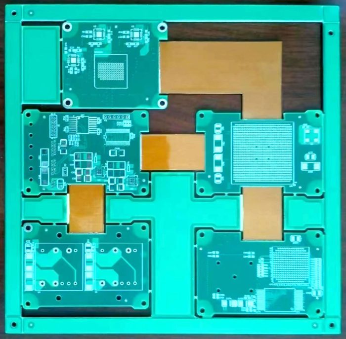
Not all PCB materials are created equal—and the material you choose can drastically influence the performance, durability, and cost of your final board. This is especially critical for industries like automotive, aerospace, LED lighting, and IoT, where reliability under specific conditions is non-negotiable.
This is the most widely used circuit board substrate. It’s a glass-reinforced epoxy laminate that offers good electrical insulation, mechanical strength, and heat resistance—suitable for most consumer electronics and industrial devices.
For applications with high thermal loads or lead-free soldering, high-TG (glass transition temperature) materials are necessary. They resist delamination and warping at elevated temperatures, making them perfect for automotive and industrial controls.
This is your go-to for high-temperature and flexible PCBs. Polyimide boards can handle extreme environments and mechanical bending—ideal for aerospace, military, and flex-rigid applications.
Need ultra-low signal loss for high-frequency RF or microwave circuits? Rogers materials and PTFE-based laminates (like Teflon) offer exceptional dielectric properties and low loss but come at a premium price and are harder to process.
Here’s a quick breakdown:
| Material | Applications | Key Properties | Drawbacks |
|---|---|---|---|
| FR4 | General electronics | Cost-effective, stable | Not ideal for high-frequency |
| High-TG FR4 | Industrial, automotive | Higher thermal reliability | Slightly more expensive |
| Polyimide | Aerospace, flex PCBs | Flexible, heat-resistant | Costly, complex handling |
| Rogers/PTFE | RF, microwave, 5G, radar | Low Dk, low loss, high frequency | Expensive, special processing |
Imagine designing a PCB for a 5G base station. You wouldn’t want to use standard FR4 because it can’t maintain signal integrity at 20 GHz. Similarly, if you’re prototyping a wearable device, you might choose polyimide for its flexibility and resistance to thermal cycling.
What’s the real story?
Choosing the wrong material can result in field failures, customer dissatisfaction, and expensive redesigns. Talk to your PCB supplier—like Jerico Multilayer PCB—to get expert recommendations based on your specs.
This is where it gets interesting…
Etching is the moment of truth in circuit board manufacturing. It’s where your brilliant design is physically carved onto copper layers to bring your circuit to life. Every misstep here? It’s costly—both in yield and functionality.
So how does it work?
Etching is the process of removing unwanted copper from the laminate to leave behind only the traces, pads, and features designed in your Gerber files. There are two main types:
The most traditional and widely used technique, wet etching involves immersing the copper-clad board in a chemical solution, typically ferric chloride, ammonium persulfate, or cupric chloride. This dissolves the exposed copper, leaving the protected traces intact.
The accuracy of wet etching heavily depends on the uniformity of the photoresist application and exposure. Overetching can reduce trace width, while underetching can lead to shorts and unconnected paths.
Used in advanced applications, this process uses ionized gas or plasma to precisely remove copper. It’s more expensive but delivers higher resolution and cleaner results—perfect for HDI circuit boards or RF applications where signal purity matters.
Let’s compare both:
| Etching Type | Cost | Resolution | Use Cases | Limitations |
|---|---|---|---|---|
| Wet Etching | Low | Moderate | Mass production, FR4 | Less precise, under/overetch risk |
| Dry Etching | High | Very high | HDI, RF, microwave boards | Expensive, slower throughput |
To control etching precision, manufacturers use an etch factor—the ratio of etch depth to lateral etching. A lower etch factor helps ensure that the copper traces remain crisp and within tolerance, especially important for fine-pitch designs.
Before moving to drilling, always inspect the board. Many manufacturers utilize AOI (automated optical inspection) right after etching to verify trace integrity, spacing, and copper pattern conformity. After all, this layer is the electrical highway of your entire design.
Up next, we’ll dive into drilling—because even a perfect circuit path is useless without properly placed vias and through-holes. Let’s go!
No matter how perfectly you’ve etched your copper traces, they’re practically useless without the proper connection points—enter circuit board drilling. This stage defines how signals move between layers and how your components get soldered into place.
There are two key purposes of drilling in circuit board manufacturing:
Creating through-holes for component leads and connectors
Establishing vias that link different circuit layers
This is the most common method, using ultra-fine carbide drill bits rotating at 100,000 RPM or more. These drills can create holes as small as 0.15mm, perfect for through-hole components and standard vias.
However, mechanical drilling has limitations—mainly tool wear and precision issues at extremely small diameters. That’s why…
For microvias or HDI designs, CO2 or UV lasers are used. These are non-contact and can create extremely fine holes under 0.1mm with very little mechanical stress on the board. Laser drilling is essential for smartphones, wearables, and medical devices where miniaturization is critical.
Let’s compare:
| Drilling Type | Min Hole Size | Speed | Ideal For | Limitations |
|---|---|---|---|---|
| Mechanical Drill | ~0.15mm | High | Through-holes, standard vias | Bit wear, less microvia usage |
| Laser Drill | <0.10mm | Moderate | HDI, microvias, small boards | Cost, setup complexity |
Now, don’t miss this…
Proper drilling also means proper annular ring management. That’s the copper pad surrounding the drilled hole—if it’s too small, your hole might miss the pad entirely. Industry standards (like IPC-2221) require at least 0.05mm of copper ring for secure connections.
And don’t forget the aspect ratio—the depth-to-diameter of your holes. A typical limit is 10:1; exceeding this could result in poor plating and connectivity failures.
Before moving on, ensure all holes pass x-ray or AOI testing. One misaligned via could mean a non-functional board in the field.
So far, you’ve drilled thousands of precise holes into your circuit board—but they’re still just empty tunnels. To make them function electrically, you need to plate them with copper. This step transforms mechanical holes into conductive vias, capable of carrying signals between layers.
Plated Through Holes (PTH) are what make multilayer boards possible. Without plating, your vias are like disconnected islands—no communication, no circuit. That’s why this step is arguably the spinal cord of PCB interconnectivity.
Here’s what really happens:
Pre-treatment cleaning – Removes drill debris and prepares hole walls for plating.
Electroless copper deposition – A thin layer of copper (~1μm) is chemically deposited inside the holes.
Electrolytic copper plating – This adds a thicker copper layer (~20–25μm) via current-driven electroplating.
But wait, there’s more…
Uniform copper distribution is tricky. circuit board designs with dense inner layers or large panels require thieving patterns to avoid over- or under-plating in certain areas.
| Step | Function | Typical Thickness | Notes |
|---|---|---|---|
| Cleaning | Prepare surface and holes | – | Removes dust and oxide |
| Electroless Plating | Base copper in holes | ~1μm | No electricity used |
| Electrolytic Plating | Thickens copper in holes/traces | 20–25μm | Controlled by current and time |
If your copper plating is inconsistent, it can lead to intermittent signal failures—the worst kind of issue for OEMs and engineers. That’s why high-end circuit board shops like Jerico Multilayer PCB invest in pulse plating and automatic thickness measurement systems.
After all the precision drilling and copper plating, your circuit board is functional—but still vulnerable. Exposed copper traces can oxidize, short-circuit, or suffer damage during soldering. That’s why the solder mask is so important—it acts like armor for your PCB.
The solder mask is the colored lacquer-like layer (often green, but also red, blue, black, or white) that’s applied to the circuit board surface to insulate and protect the copper traces. Only the component pads are left exposed for soldering.
There are two primary types of solder mask application:
Liquid Photoimageable (LPI) – The most common method for professional circuit boards. It’s screen printed or sprayed on, then exposed and developed with UV light to define pad openings.
Dry Film Solder Mask – Used for very high-precision or rigid-flex boards, applied using vacuum lamination.
The alignment of the solder mask is critical. If the openings don’t line up precisely with the pads, soldering becomes a nightmare. That’s why CCD camera-guided exposure machines are essential for modern production lines.
| Color | Visibility | Heat Resistance | Common Uses |
|---|---|---|---|
| Green | Excellent | High | Default for all circuit boards |
| Black | Low | Moderate | Consumer & automotive |
| Red | Moderate | High | High-visibility applications |
| Blue | Moderate | Moderate | LED & industrial electronics |
| White | Low | Low | LED backlighting, cosmetics |
Solder mask isn’t just for looks—it protects the board from corrosion, accidental bridging, and handling damage. It also makes automated soldering like reflow or wave soldering possible by keeping solder where it belongs.
And here’s a secret most newcomers miss…
Glossy vs. matte solder mask finishes can impact AOI (Automated Optical Inspection). Matte reduces reflections and improves image clarity during testing.
Ready for the good part?
Your PCB may be electrically sound and physically protected, but without clear labeling, it’s like a map without street names. That’s where silkscreen printing comes in—it adds all the critical visual information needed for assembly and troubleshooting.
Silkscreen, also called legend printing, is the process of printing component identifiers, logos, polarity marks, test points, and version numbers directly onto the board surface. It’s the white (or sometimes yellow) text you see on top of the solder mask.
Here’s the real story…
The silkscreen isn’t just for looks—it’s a powerful functional guide. A well-marked board can dramatically reduce assembly errors, simplify repairs, and improve user confidence. On the flip side, a poorly printed silkscreen—or none at all—can turn a high-quality board into a costly puzzle.
| Method | Description | Pros | Cons |
|---|---|---|---|
| Manual Screen Print | Stencil and ink applied by hand | Cost-effective | Low resolution, slow |
| Liquid Inkjet | Ink sprayed by a printer head | Fast and automated | Limited ink types |
| UV LED Printing | High-resolution UV-curable ink | Sharpest results | Higher equipment cost |
Font size and line width matter. Most manufacturers require 0.15 mm line width minimum and font height ≥ 1.0 mm to ensure readability. If text overlaps with pads or vias, it will be removed during manufacturing, so smart layer management in your PCB design tool is essential.
Many OEMs also use silkscreen to include QR codes or barcodes for traceability. In some industries—such as aerospace or medical—it’s even a regulatory requirement.
So don’t underestimate this step. While it may seem cosmetic, silkscreen printing transforms your PCB from a technical prototype into a polished, professional-grade product.
This is where it gets interesting…
Even the most perfectly designed and precisely fabricated PCBs can fail—if they aren’t tested properly. Testing is not an optional extra; it’s the last barrier between your customer and a non-functional product. Let’s talk about how manufacturers ensure every board meets the mark.
Quality control prevents shipping defective boards that can lead to:
● Product recalls
● Loss of customer trust
● Damage to end-use equipment
● Costly rework or scrap
To avoid this, manufacturers apply both electrical and visual inspection techniques at multiple stages.
| Test Type | Purpose | Method | Notes |
|---|---|---|---|
| Flying Probe Test | Verifies electrical continuity | Automated probes test nets | Ideal for small volumes |
| In-Circuit Test (ICT) | Functional component testing | Custom fixture-based test setup | Great for mass production |
| Automated Optical Inspection (AOI) | Checks solder mask, silkscreen, alignment | Cameras scan for errors | Fast, reliable visual QC |
| X-Ray Inspection | Verifies inner layers, BGA joints | Non-destructive, 3D imaging | Used in high-end applications |
| Functional Testing | Validates full circuit performance | Inputs and outputs verified | Simulates end-use conditions |
But here’s the kicker…
Testing is only effective when paired with robust documentation and traceability. Professional PCB manufacturers assign serial numbers or QR codes to each board batch, recording lot number, production date, and inspection results. This supports root cause analysis and warranty control.
Some companies even implement burn-in testing, running boards under high temperature and voltage to catch early-life failures—vital for aerospace, defense, and automotive PCBs.
Once tested, compliant PCBs receive a final inspection pass label, including inspector ID and date. Failed boards are either reworked (if possible) or discarded following internal quality procedures.
Smart manufacturers also use Statistical Process Control (SPC) to monitor trends and prevent issues before they start.
So, whether you’re producing 50 or 50,000 units, testing is your insurance policy for performance and reputation.
What’s the real story?
Making a PCB board isn’t just about etching copper on a laminate—it’s about precision, planning, and performance. Every stage, from schematic design to final inspection, plays a critical role in ensuring the board functions flawlessly in its intended environment.
We’ve walked through the entire journey of how to make a express PCB board:
Starting from design and material selection
Diving into etching, drilling, and layer stacking
Applying solder masks and silkscreens
Finishing with robust testing protocols
Each section matters. A small error in one step can compromise the entire circuit board. But when done right? It results in a high-quality, reliable product ready for integration into everything from consumer electronics to mission-critical aerospace systems.
Here’s the bottom line: whether you’re an engineer, buyer, or manufacturer, understanding the full lifecycle of a circuit board board gives you an edge. You’ll communicate better with your suppliers, set clearer expectations, reduce cost overruns, and—most importantly—deliver quality consistently.
Jerico Multilayer PCB provides state-of-the-art PCB manufacturing with a strong focus on precision and quality. With our expert team and advanced technology, we ensure your PCBs meet the highest standards. Contact us for your next PCB project and experience reliable service.
Q1: What is a PCB board?
A PCB (Printed Circuit Board) is a flat board that connects electronic components using conductive pathways etched from copper sheets. It provides structure and electrical connectivity in virtually all modern electronic devices.
Q2: How does the circuit board manufacturing process work?
It starts with a circuit design, followed by material selection, layer buildup, etching, drilling, and surface finishing. The process concludes with testing and inspection to ensure quality and functionality.
Q3: Can I make a PCB board at home?
Yes, for simple prototypes. DIY methods include toner transfer, UV exposure, and chemical etching. However, they are limited in complexity and accuracy compared to industrial manufacturing.
Q4: What materials are used to make a PCB?
Common materials include FR-4 (fiberglass epoxy laminate), copper foil for traces, solder masks, and silkscreen inks. Advanced boards may use ceramics, polyimide, or aluminum substrates.
Q5: How long does it take to manufacture a PCB?
Lead times vary by complexity and volume. Standard boards take 3–7 days, while expedited services offer delivery within 24–72 hours. Complex multilayer boards may require longer.


Connect to a Jerico Multilayer PCB engineer to support your project!
Request A Quote


 Quote
Quote