


 Well-known PCB supplier
+86 13603063656
After 25 years in PCB manufacturing and failure analysis, I have become increasingly convinced of one thing:
For most electronic applications, 1.6mm remains the most reliable PCB thickness.
Not because it is “traditional”.
But because it provides the best balance between:
Many engineers focus primarily on:
However, PCB thickness itself has a major influence on long-term reliability, especially in multilayer PCB structures.
1.6mm PCB Thickness
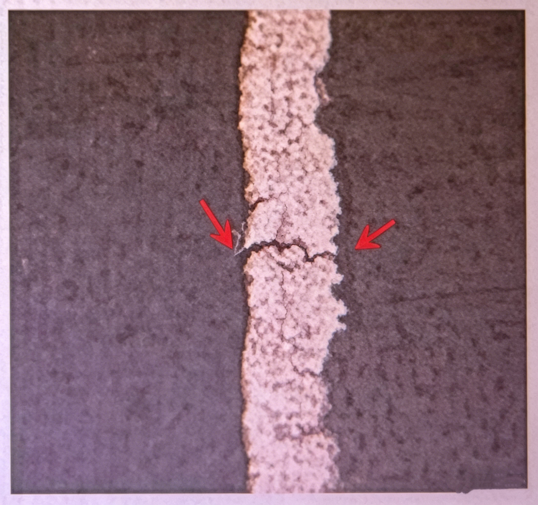
One of the most underestimated reliability risks in PCB manufacturing is Z-axis thermal expansion.
Copper vias and FR-4 materials expand very differently during thermal cycling.
Typical CTE values:
Copper:
~17 ppm/°C
Standard FR-4 Z-axis expansion:
250 ppm/°C above Tg
This mismatch creates cyclic mechanical stress inside plated through holes during:
Over time, this stress can lead to:
The thicker the PCB, the greater the accumulated Z-axis expansion.
As PCB thickness increases, stress inside plated vias also increases significantly.
Many thick multilayer PCBs can successfully pass:
Yet still fail later during real-world operation.
This is because laboratory qualification tests often cannot fully simulate years of thermal cycling under actual field conditions.
In real manufacturing experience, thick PCBs frequently show increased long-term via reliability risks, especially in:
In some cases, boards may operate normally for months or years before intermittent failures begin appearing.
This type of failure is particularly dangerous because it is often:
In our own failure analysis experience, we have handled cases where thick multilayer server boards passed qualification testing but later developed PPM-level via failures after prolonged service operation.
Some engineers assume:
“Thinner PCBs must always be more reliable because thermal stress is lower.”
This is not entirely correct.
While thinner PCBs reduce thermal expansion stress, they also lose mechanical rigidity.
This introduces different reliability risks, including:
In many situations, these latent defects cannot even be detected during electrical testing before shipment.
The PCB passes inspection,
but field failures appear later during customer assembly or operation.
Therefore, reliability is not simply about making the PCB thinner.
It is about achieving the correct engineering balance.
There is a reason why 1.6mm became the global mainstream PCB thickness.
It was not accidental.
1.6mm provides an excellent balance between:
Even today, more than 80% of our production remains 1.6mm thickness.
Many automotive and industrial electronics applications also continue to rely heavily on 1.6mm structures for long-term reliability consistency.
In real manufacturing environments, reliability is usually achieved through balanced and proven structures rather than theoretical optimization.
One important misconception in the PCB industry is:
Passing IPC testing does not always guarantee long-term field reliability.
A PCB may successfully pass:
and still develop failures later in customer applications.
The true challenge is not simply passing laboratory qualification.
The real challenge is surviving years of thermal cycling and mechanical stress in actual field operation.
This is why some PCB failures only appear:
These delayed reliability failures are often the most expensive and difficult problems in the electronics industry.
From a PCB manufacturing reliability perspective:
PCB thickness above 2.0mm should generally be avoided unless structurally necessary.
If thicker PCBs are unavoidable, additional reliability controls become extremely important.
Recommended controls include:
Because thicker PCB structures naturally create higher long-term via reliability risk.
In PCB manufacturing, reliability is not achieved by pushing structures to theoretical limits.
It is achieved by staying within stable and proven engineering boundaries.
After decades of manufacturing and failure analysis experience, 1.6mm PCB thickness still remains one of the safest and most reliable balances between:
For most industrial and automotive electronic applications, 1.6mm continues to be the industry’s most practical and reliable PCB thickness choice.
This topic also generated extensive engineering discussion on LinkedIn among PCB manufacturing and reliability professionals.
For additional industry perspectives and discussion, you can also read the original LinkedIn technical post by Tony Niu.


Connect to a Jerico Multilayer PCB engineer to support your project!
Request A Quote
 Quote
Quote
 E-mail
 Whatsapp