


+86 13603063656

When engineers evaluate materials for high-performance electronics, Copper vs. Gold is a comparison that frequently surfaces. These metals have been central to PCB (Printed Circuit Board) manufacturing, RF (Radio Frequency) designs, and advanced high-speed digital circuits. While both materials are exceptional conductors, their subtle differences in electrical properties, thermal behavior, corrosion resistance, and manufacturing cost can dramatically influence a design’s long-term reliability and performance.
In the context of effective permittivity — the interaction between an electromagnetic field and a conductive surface — material choice is not purely about conductivity. Instead, it involves understanding how the metal behaves in the real environment of a PCB trace, microstrip, or waveguide. Here, the goal is not simply to select “the better metal” but rather to choose the one that aligns with your design’s frequency range, environmental constraints, and cost-performance targets.
In this article, we will systematically explore Copper vs. Gold, comparing their physical and electrical characteristics, examining their advantages, and detailing the manufacturing processes used in PCB applications. We will also touch on real-world examples from aerospace, medical, and consumer electronics to illustrate practical decision-making in material selection.
Copper vs. Gold
Effective permittivity is a parameter that defines how an electric field interacts with both the conductive material and the dielectric substrate in a PCB or electronic device. While the dielectric constant (Dk) is a property of the substrate, the conductor’s surface characteristics can subtly alter the propagation speed of signals — particularly at high frequencies.
In Copper vs. Gold comparisons, the difference in effective permittivity comes not from bulk electrical conductivity alone but from factors like:
Surface Roughness — A smoother surface can reduce the effective dielectric constant seen by the signal.
Skin Depth Effects — At high frequencies, current flows primarily on the conductor’s surface. Gold, with slightly different resistivity and smoother plated finishes, can influence signal propagation.
Oxidation Resistance — Copper oxidizes over time, potentially increasing surface roughness and changing signal characteristics. Gold remains stable, which can make effective permittivity more predictable in the long term.
By understanding these effects, designers can optimize their choice of metal for performance-critical applications such as 5G base stations, aerospace navigation systems, and high-speed server interconnects.
The story of Copper vs. Gold in electronics is a narrative of balancing cost, performance, and manufacturability. Copper has been the backbone of electrical wiring and PCB manufacturing since the earliest printed circuit designs in the 1950s. Its high conductivity, relatively low cost, and ease of electroplating made it the natural choice for mass production.
Gold, on the other hand, emerged in high-reliability applications — space electronics, military systems, and medical implants — where corrosion resistance and long-term stability were more important than raw cost. Initially used in thin layers as a plating over copper traces, gold’s role expanded in the late 20th century with the rise of fine-pitch connectors, microelectronics, and high-frequency RF circuits.
Today, Copper vs. Gold is less a battle of “which is better” and more about “which is right for the job.” While copper dominates in most cost-sensitive markets, gold retains a stronghold in specialized high-value sectors.
When comparing Copper vs. Gold for PCB and high-frequency design, it is important to move beyond their market reputations and examine the measurable physical and chemical properties that directly influence performance. Both metals have excellent electrical conductivity, but their other characteristics differ in ways that can significantly impact long-term functionality.
Key Physical Properties Table:
| Property | Copper | Gold |
|---|---|---|
| Electrical Conductivity (S/m) | ~5.96 × 10⁷ | ~4.10 × 10⁷ |
| Thermal Conductivity (W/m·K) | ~401 | ~317 |
| Density (g/cm³) | ~8.96 | ~19.3 |
| Melting Point (°C) | ~1,085 | ~1,064 |
| Corrosion Resistance | Moderate (oxidizes easily) | Excellent (does not oxidize) |
| Surface Smoothness (plated) | Good | Excellent |
From this table, it is clear that copper has higher electrical and thermal conductivity than gold, making it the more efficient conductor in raw performance terms. However, gold’s corrosion resistance and chemical stability give it an advantage in environments where oxidation could affect signal integrity over time.
Design Implication:
In high-frequency circuits, the difference in surface oxidation resistance can outweigh bulk conductivity advantages. For example, a gold-plated contact pad will maintain stable RF characteristics for years without tarnishing, whereas bare copper would require protective coatings to achieve similar performance.
Electrical conductivity is often the first metric designers think about when evaluating metals for PCB conductors. On paper, Copper vs. Gold is not a close race: copper’s conductivity is about 45% higher. This means that for the same cross-sectional area, copper can carry more current with less resistive loss.
However, in high-frequency applications, where the skin effect confines current to the conductor’s surface, surface condition becomes equally important. Gold’s resistance to tarnish ensures that its surface remains highly conductive over time, whereas copper’s oxide layer increases surface resistance.
Example Calculation:
A 10 GHz signal on a microstrip line will have a skin depth of approximately 0.65 μm in copper and 0.78 μm in gold.
If the copper surface has oxidized, the effective resistance can increase, causing additional signal loss.
Gold plating (usually over nickel) ensures stable surface conductivity regardless of storage or operating environment.
Practical Engineering Choice:
If you are designing for low-cost, short-lifespan consumer devices, copper is usually the go-to choice. For aerospace, medical, or defense electronics, gold plating on contact surfaces can justify the higher material cost due to reliability benefits.
Thermal conductivity is critical in high-power electronics, especially where heat dissipation determines performance and reliability. Copper’s thermal conductivity is roughly 26% higher than gold’s, meaning it can more efficiently transfer heat away from high-power components.
Copper Advantages in Thermal Management:
Effective in power electronics, RF power amplifiers, and LED substrates.
Allows for smaller thermal vias and less aggressive heatsinking.
Reduces hot spot formation under high continuous loads.
Gold’s Role in Thermal Performance:
Gold is rarely used for bulk thermal conduction in PCBs due to cost and density, but its thermal stability and chemical inertness make it valuable in thin-layer applications where surface stability is as important as heat transfer.
Example:
In a high-power microwave amplifier, copper heat spreaders are often gold-plated to protect against oxidation while still relying on copper for the majority of thermal dissipation.
Corrosion resistance is where gold decisively outperforms copper. Bare copper oxidizes within hours of exposure to air, forming a thin layer of copper oxide. While this layer is not always catastrophic for DC conduction, it can severely affect RF performance and solderability.
Gold’s Corrosion Advantages:
Does not oxidize or tarnish, even in high-humidity or corrosive environments.
Provides stable, predictable electrical performance over decades.
Allows for high-reliability contact surfaces in connectors and switch contacts.
Copper’s Protection Methods:
Immersion tin or immersion silver coatings.
ENIG (Electroless Nickel Immersion Gold) finish — a hybrid approach where copper traces are plated with nickel and then gold for surface protection.
Conformal coatings to seal copper from air and moisture.
Surface finish plays a decisive role in ensuring that the underlying copper or gold delivers its intended electrical and mechanical performance throughout the product’s lifecycle. In Copper vs. Gold PCB fabrication, the surface finish selection can influence not only effective permittivity but also solderability, contact resistance, and wear resistance.
Common Surface Finish Types:
Bare Copper (OSP – Organic Solderability Preservative)
Cost-effective option for short-lifespan products.
Provides a temporary protective layer to prevent oxidation before soldering.
Not suitable for high-frequency designs where long-term surface stability is critical.
ENIG (Electroless Nickel Immersion Gold)
Combines copper conductivity, nickel as a diffusion barrier, and a thin layer of gold for oxidation resistance.
Excellent for fine-pitch components, BGA pads, and RF signal integrity.
Common in aerospace and high-reliability applications.
Hard Gold Plating
Thicker and more durable gold layer than ENIG.
Ideal for edge connectors, switch contacts, and wear-prone areas.
Higher cost due to greater gold usage.
Immersion Silver or Immersion Tin
Better than bare copper for corrosion protection, but not as stable as gold.
Cost-effective middle ground for consumer electronics.
Design Insight:
For high-frequency boards, ENIG is often the sweet spot in the Copper vs. Gold debate, providing stable electrical performance without the excessive cost of hard gold. For designs with mechanical wear points, hard gold is unmatched.
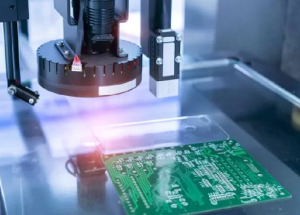
The manufacturing sequence for Copper vs. Gold PCBs involves multiple stages where precision and process control determine the final product’s reliability. The choice between copper and gold affects plating steps, process complexity, and cost.
Typical PCB Fabrication Flow with Copper:
Copper Clad Laminate Preparation – Base FR-4 or advanced substrate with copper foil.
Patterning – Photoresist application, exposure, and development to define circuit traces.
Etching – Removal of unwanted copper.
Surface Finish – OSP, immersion tin, immersion silver, or ENIG plating.
Additional Steps for Gold Integration:
Nickel Barrier Plating – Applied to prevent copper diffusion into gold.
Gold Deposition – Immersion gold for ENIG, or electrolytic gold for hard plating.
Selective Plating Masking – For areas requiring gold only (e.g., connector fingers).
Manufacturing Impact:
Gold integration adds both time and cost to the process but can be essential for performance-critical designs.
From a procurement perspective, Copper vs. Gold decisions are heavily influenced by both raw material pricing and global supply chain stability.
Copper Cost Dynamics:
More stable and widely available.
Prices fluctuate with industrial demand (construction, power distribution, automotive).
Recyclable at scale, which moderates long-term price volatility.
Gold Cost Dynamics:
Subject to global financial market trends as a precious metal.
Prices are generally much higher per gram than copper — often hundreds of times more.
Used in extremely small amounts for PCB plating, so cost impact is tied to plating thickness and coverage area.
Strategic Sourcing Considerations:
Hybrid approach (copper bulk, gold plating only on critical areas) is the most common in high-performance PCB design.
In volatile gold markets, design engineers may adjust plating thickness or coverage to balance cost and performance.
Manufacturers with in-house plating capabilities, like JM PCB, can respond faster to market fluctuations by adjusting process parameters without impacting delivery schedules.
Choosing between Copper vs. Gold is not about finding the “better” metal, but selecting the one that aligns with your design’s performance, cost, and longevity requirements:
Copper: Excellent electrical and thermal conductivity, cost-effective, suitable for most consumer electronics and high-power applications. Requires protective finishes to mitigate oxidation for long-term reliability.
Gold: Superior oxidation resistance, smooth surface, predictable high-frequency performance, biocompatible for medical applications. Ideal for connectors, contact pads, and high-speed signal launch areas.
For most modern designs, a hybrid approach — copper traces with selective gold plating — achieves the optimal balance between performance and cost. Ultimately, understanding effective permittivity, surface roughness, oxidation behavior, and manufacturing constraints allows engineers to make informed decisions. By combining simulation insights with practical manufacturing strategies, designers can maximize signal integrity, minimize losses, and ensure reliable operation over the entire product lifecycle.
Q1: What is the difference between rolled copper foil and electrolytic copper foil?
A: Rolled copper foil is produced by mechanically rolling copper into thin sheets, offering superior surface smoothness, mechanical strength, and uniform thickness. It is ideal for high-frequency and high-density designs because the smoother surface reduces signal loss and improves effective permittivity stability. Electrolytic copper foil, on the other hand, is deposited via an electrolytic process. It is more flexible, easier to handle, and generally more cost-effective, but its rougher surface can slightly increase conductor loss at very high frequencies.
Q2: How does copper vs. gold affect effective permittivity in PCB designs?
A: The effective permittivity of a PCB trace is influenced not only by the dielectric material but also by the conductor surface. Copper with rough or oxidized surfaces slightly increases effective permittivity, which can slow signal propagation and alter impedance. Gold, being chemically inert and smooth when plated, maintains lower and more stable effective permittivity over the device lifetime. For high-frequency and high-speed designs, gold plating on copper can minimize permittivity variations and improve signal integrity.
Q3: How does copper oxidation affect signal quality compared to gold?
A: Copper oxidation creates a thin layer of copper oxide, which is less conductive and has higher dielectric constant. This layer can increase signal attenuation, cause impedance mismatch, and reduce solderability. Gold does not oxidize, ensuring stable contact resistance and preserving high-frequency signal integrity. In designs requiring decades of reliability, gold plating on copper traces or contacts ensures predictable electrical performance even in harsh environments.
Q4: What is the difference between selective gold plating and full gold plating?
A: Selective gold plating applies gold only to critical areas, such as contact pads, edge connectors, or high-frequency launch points, while leaving the rest of the copper traces unplated. Full gold plating covers all conductive surfaces, offering maximal corrosion protection but at a significantly higher cost. Selective plating is preferred in cost-sensitive high-frequency or high-reliability applications because it provides the benefits of gold where it matters most without excessive material use. Manufacturers like JM PCB specialize in selective plating to balance performance and cost.
Q5: How does metal choice impact long-term impedance stability?
A: Long-term impedance stability is influenced by conductor surface condition, oxidation, and thermal cycling. Copper-only surfaces may develop oxidation over time, slightly increasing impedance. Gold-plated surfaces resist chemical changes, providing consistent conductor-dielectric interaction and maintaining the designed impedance over years. For high-speed or RF applications where even minor impedance shifts can degrade performance, gold plating on copper traces or contact points ensures predictable long-term stability.


Connect to a Jerico Multilayer PCB engineer to support your project!
Request A Quote


 Quote
Quote