


+86 13603063656
In modern electronics, printed circuit boards (PCBs) represent the backbone of nearly every device, from consumer gadgets to advanced aerospace systems. The way PCBs are manufactured has evolved dramatically over the past decades, with High-Volume PCB production emerging as a critical enabler for both efficiency and reliability in global supply chains. While many discussions of manufacturing focus on cost savings, this article explores the deeper advantages of High-Volume PCB production, particularly its role in ensuring stable supply, consistent quality, and long-term partnerships between manufacturers and end-users.
The objective here is not only to provide a detailed technical explanation of what High-Volume PCB production entails but also to examine the broader implications it carries for industries seeking resilience in uncertain times. In addition, personal reflections are included to highlight how this topic intersects with real-world challenges in supply chain management and technology strategy.
At its core, High-Volume PCB production refers to the large-scale manufacturing of circuit boards in quantities ranging from tens of thousands to millions of units. This type of production is typically executed by specialized facilities equipped with advanced automated equipment, large production floors, and robust quality management systems. Unlike prototype or small-batch manufacturing, High-Volume PCB operations must balance efficiency, repeatability, and tight tolerances to ensure that every unit meets stringent requirements.
The process often involves:
Automated panelization for optimizing material usage.
High-speed drilling and routing for consistent hole precision.
Mass lamination cycles to handle multilayer designs at scale.
Automated Optical Inspection (AOI) and testing to guarantee defect-free boards.
In essence, High-Volume PCB manufacturing is less about flexibility for one-off designs and more about delivering massive quantities with unwavering consistency.

High-Volume PCB
While the initial attraction to High-Volume PCB production often stems from cost savings through economies of scale, the benefits extend far beyond financial considerations.
Reliability of Supply – Manufacturers can align production with predictable schedules, reducing lead-time variability.
Consistent Quality – Advanced automation minimizes human error and ensures boards remain within tight specifications.
Global Scalability – High-Volume PCB enables companies to roll out new products across international markets quickly.
Material Efficiency – Large orders allow better negotiation with raw material suppliers, ensuring stable access to copper foils, laminates, and resins.
Design Standardization – High volumes push engineering teams to refine designs for manufacturability, indirectly improving long-term product reliability.
These advantages mean that High-Volume PCB is not merely a cost-saving tactic but a foundation for building resilient, trusted supply chains.
The relationship between High-Volume PCB production and supply chain reliability can be viewed from three angles: capacity assurance, risk mitigation, and vendor partnerships.
Capacity Assurance: Large-scale facilities can adapt production volumes to demand spikes without sacrificing delivery schedules.
Risk Mitigation: By maintaining rigorous quality control, High-Volume PCB reduces the risks of field failures, warranty claims, and recalls.
Vendor Partnerships: Long-term relationships with suppliers of laminates, copper foil, and chemicals strengthen resilience against material shortages.
For companies managing global supply chains, these benefits translate into fewer disruptions and more predictable growth trajectories.
When analyzing the technical aspects of High-Volume PCB manufacturing, several critical factors emerge:
Copper Foil Selection – Choosing between rolled copper foil and electrolytic copper foil has major implications for board performance.
Laminate Properties – Material properties such as Tg (glass transition temperature) affect durability in high-performance applications.
Solder Mask Uniformity – In mass production, ensuring even coverage is essential to avoid defects.
Testing Protocols – Flying probe and in-circuit testing systems must be integrated into the workflow.
These considerations highlight the complexity behind High-Volume PCB operations, underscoring why only experienced manufacturers can execute them reliably.
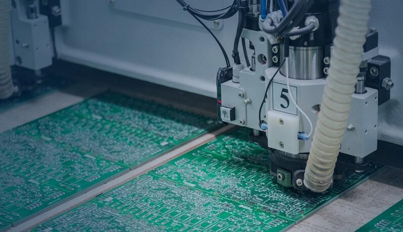
Understanding the workflow of High-Volume PCB production is essential for appreciating why it plays such a central role in building supply chain reliability. Unlike small-batch fabrication, where manual intervention is often acceptable, high-volume environments rely on automation, repeatability, and process optimization.
The process begins with transferring the final design files into a format optimized for high-volume manufacturing. At this stage, engineers:
Verify Design for Manufacturability (DFM) compliance.
Panelize boards to reduce material waste and streamline assembly.
Create tooling and production guidelines to ensure consistency.
High-Volume PCB manufacturing requires large-scale lamination cycles, where multiple layers are pressed together under high heat and pressure. Materials must be managed efficiently to prevent contamination. Even small errors at this stage could compromise thousands of units.
High-speed CNC drilling machines operate simultaneously across multiple panels, ensuring precision in thousands of vias. Electroplating follows, depositing copper into holes and across layers. This is where supply chain reliability connects with technical execution: stable copper chemistry and bath consistency must be maintained across massive production runs.
Automated photolithography machines apply and expose imaging resists, followed by controlled etching. High-Volume PCB etching must strike a balance between speed and accuracy—etching too aggressively can cause over-etching across all units, while under-etching risks shorts.
Applying solder mask consistently across thousands of panels demands precise ink deposition, curing, and inspection. Surface finishing (ENIG, HASL, OSP, etc.) is applied in bulk, and consistency here ensures reliable solderability during assembly.
No matter how automated the process, testing is non-negotiable. In high-volume operations:
Automated Optical Inspection (AOI) screens for defects.
Flying probe or in-circuit testing validates electrical performance.
Statistical Process Control (SPC) ensures quality metrics remain stable across millions of units.
The choice of materials directly affects supply chain resilience. For High-Volume PCB production, manufacturers must not only ensure performance but also secure reliable access to raw materials.
Copper Foils: Rolled vs electrolytic copper foil selection impacts signal integrity, mechanical strength, and cost-effectiveness. Large orders require long-term supplier contracts.
Laminates: High-Tg FR4, polyimide, or high-frequency substrates must be sourced in predictable volumes.
Solder Masks: UV-curable inks must meet environmental and RoHS standards while being available in bulk.
Chemicals: Plating baths, etching solutions, and cleaning agents require robust logistics to avoid disruptions.
Supply Chain Note: During global material shortages (e.g., copper price spikes), companies relying on High-Volume PCB partners with established supplier networks were better positioned to maintain delivery schedules.
High-Volume PCB production is the hidden enabler of modern electronics. Its impact spans industries:
Consumer Electronics
Smartphones, tablets, and wearables rely heavily on multi-layer High-Volume PCB production. Timely launches of flagship devices depend on millions of defect-free boards arriving exactly on schedule.
Automotive
Vehicles increasingly integrate advanced driver-assistance systems (ADAS), infotainment, and EV battery management, all powered by high-reliability PCBs. High-Volume PCB ensures consistency across production lines where safety is critical.
Telecommunications
5G infrastructure and data centers demand PCBs with low-loss laminates and precise impedance control. Scaling up production allows telecom providers to roll out global networks faster.
Medical Devices
Reliability is paramount in medical electronics. High-Volume PCB partners who maintain rigorous certification standards (ISO 13485, IPC Class 3) ensure patient safety while meeting large order volumes.
Industrial and Aerospace
Even in sectors with relatively lower volume compared to consumer electronics, batch reliability ensures long-term mission success and reduced field failures.
While the advantages of High-Volume PCB production are significant, challenges remain:
Yield Management – Even small defect rates multiply when producing millions of units.
Mitigation: Advanced AOI, inline testing, and Six Sigma methodologies.
Material Volatility – Fluctuations in copper and resin prices can disrupt planning.
Mitigation: Long-term supplier contracts and diversified sourcing.
Technological Obsolescence – As devices evolve, manufacturers risk holding outdated PCBs.
Mitigation: Agile engineering and quick-turn prototyping before scaling.
Global Logistics – Shipping millions of PCBs across continents requires robust logistics.
Mitigation: Multiple production bases, regional warehouses, and predictive analytics.
The story of High-Volume PCB is more than a technical narrative. It represents the backbone of the global electronics supply chain and the silent force behind nearly every modern innovation.
Beyond Cost: While cost reduction drove the initial push for High-Volume PCB, today its role is centered on supply chain reliability.
Reliability as a Differentiator: Companies succeed not only by designing great products but by delivering them at scale with zero defects.
Strategic Resilience: In a world of geopolitical uncertainty, environmental challenges, and rapidly changing demand, resilient High-Volume PCB suppliers are strategic assets.
The Future: With AI, flexible electronics, sustainability, and new materials, High-Volume PCB will evolve into a smarter, greener, and more integrated technology.
From my perspective, the most important insight is this: electronics innovation is meaningless without reliable High-Volume PCB manufacturing. A brilliant idea can fail if the PCB supply chain cannot scale it to millions of units. In the next decade, the winners in electronics will not simply be those who innovate, but those who master the art of High-Volume PCB reliability at global scale.
1. What is the difference between rolled copper foil and electrolytic copper foil?
Rolled copper foil is produced by mechanically rolling copper into thin sheets, offering better surface quality and mechanical strength. Electrolytic copper foil is deposited via an electrolytic process and is more flexible and cost-effective.
2. Why is High-Volume PCB important for global supply chains?
High-Volume PCB ensures stable delivery schedules, consistent quality, and reduced risks of supply disruptions, making it critical for industries dependent on just-in-time operations.
3. How do manufacturers maintain quality in High-Volume PCB production?
They use automated inspection systems, strict process controls, and statistical quality management to minimize defects across thousands or millions of units.
4. Can High-Volume PCB support custom designs?
Yes, but customization is usually standardized before mass production to ensure repeatability and yield. Prototyping and pilot runs are often required before scaling up.
5. What industries benefit most from High-Volume PCB?
Consumer electronics, automotive, telecommunications, and medical devices are key sectors that rely heavily on large-scale PCB manufacturing.


Connect to a Jerico Multilayer PCB engineer to support your project!
Request A Quote


 Quote
Quote