


+86 13603063656
2-Layer Flexible Circuits represent a unique class of printed circuit boards (PCBs) designed to combine mechanical flexibility with high electrical performance. Unlike traditional rigid PCBs, which are constrained to flat, inflexible substrates, 2-Layer Flexible Circuits can bend, fold, or twist without compromising the continuity of electrical connections. This capability opens doors to compact, high-density designs, especially where space and weight constraints are critical, such as in wearable electronics, medical devices, and aerospace applications.
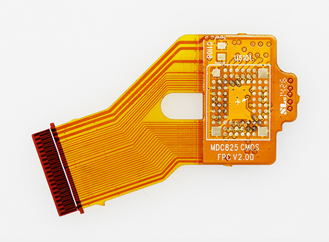
Structurally, a 2-Layer Flexible Circuit consists of two conductive layers, typically made from copper foil, separated by an insulating dielectric material such as polyimide. The layers are interconnected using via holes or plated through-holes, enabling complex routing while maintaining a minimal footprint. By having two layers instead of one, designers can implement more sophisticated circuits, reduce routing congestion, and achieve better signal integrity in high-speed applications.
The flexibility of these circuits does not compromise reliability. Through careful material selection and advanced manufacturing techniques, 2-Layer Flexible Circuits exhibit excellent thermal stability, chemical resistance, and mechanical endurance, ensuring consistent performance even under challenging conditions.

2-Layer Flexible Circuits
The concept of flexible circuitry emerged in the mid-20th century, initially as a solution for space-constrained military and aerospace systems. Early designs relied on single-layer flexible circuits, but as electronic devices became increasingly sophisticated, the demand for higher circuit density and more reliable connections grew. This led to the evolution of multi-layer flexible circuits, with the 2-Layer Flexible Circuits being a practical and cost-effective solution for many applications.
Advancements in polyimide substrates, high-quality copper foils, and precision etching processes have driven the widespread adoption of 2-Layer Flexible Circuits across industries. Today, they are not just a niche technology but a strategic component in high-performance electronic systems, balancing flexibility, density, and reliability more effectively than single-layer or rigid PCBs.
From a strategic design perspective, 2-Layer Flexible Circuits offer unparalleled advantages in applications where traditional PCBs fail. The ability to integrate high-density circuits into flexible form factors enables engineers to rethink device architectures, optimize space utilization, and even reduce overall weight. This, in turn, can improve thermal management, reduce assembly complexity, and enhance the product’s lifecycle performance.
The foundation of any high-performance 2-Layer Flexible Circuit lies in its material composition. Selecting the right materials ensures that the circuit can withstand mechanical stress, thermal cycles, and chemical exposure without degradation. Typically, the substrate material is polyimide, which offers excellent thermal stability, high tensile strength, and chemical resistance. Polyimide allows the circuit to bend, fold, or twist repeatedly while maintaining its structural integrity.
For the conductive layers, copper foil is standard, available in two primary types: rolled copper foil and electrolytic copper foil. Rolled copper foil provides superior surface smoothness and mechanical strength, making it suitable for applications that require fine line features or enhanced durability. Electrolytic copper foil, on the other hand, is more flexible and cost-effective, ideal for circuits that require frequent bending or folding. These material choices directly influence the reliability and performance of 2-Layer Flexible Circuits.
Insulating layers or adhesives are also critical. They must bond firmly to the copper layers, resist delamination, and maintain dielectric properties over time. Advances in high-performance adhesives and lamination techniques have significantly improved the longevity and mechanical reliability of these circuits.
Designing a 2-Layer Flexible Circuit requires careful attention to routing, bend zones, and layer interconnections. Unlike rigid PCBs, the layout must account for mechanical stress during bending, especially in areas where repeated flexing occurs. Designers often define bend radius limits, ensuring the copper traces do not crack under stress.
High-density designs are achievable through two conductive layers, which allow complex signal routing without increasing the circuit footprint. Designers typically use staggered vias and crossovers to minimize signal interference and maintain electrical integrity. Layer-to-layer alignment and precise etching are crucial to avoid shorts or open circuits, which can compromise reliability.
Thermal considerations are also integral to layout design. The materials used in 2-Layer Flexible Circuits have different coefficients of thermal expansion (CTE), and improper design can lead to stress accumulation and delamination under heat cycles. Proper component placement and copper distribution help balance mechanical and thermal stresses, ensuring long-term durability.
The design of 2-Layer Flexible Circuits is both an art and a science. Beyond selecting high-quality materials, engineers must anticipate mechanical, thermal, and electrical stresses that the circuit will experience throughout its lifecycle. A well-designed 2-Layer Flexible Circuit maximizes density while minimizing risk, enabling devices that are lighter, more compact, and more reliable.
The production of 2-Layer Flexible Circuits involves a precise sequence of processes to ensure both mechanical flexibility and electrical reliability. Understanding these steps is essential for achieving high-density, high-performance designs.
Substrate Preparation:
The process begins with a polyimide substrate, chosen for its thermal stability and flexibility. The substrate is cleaned thoroughly to remove any contaminants that could compromise adhesion or electrical performance.
Copper Lamination:
Copper foil layers are laminated onto the substrate. The type of copper—rolled or electrolytic—is selected based on the circuit’s mechanical and electrical requirements. Lamination is performed under controlled heat and pressure to ensure uniform bonding without voids or delamination.
Circuit Patterning (Photolithography):
A photoresist is applied to the copper layers, and the circuit design is transferred using UV exposure. This step defines the precise pattern of conductive traces.
Etching:
Unprotected copper is removed through chemical etching, leaving behind the desired conductive paths. This step requires careful control to achieve fine line resolution and avoid undercutting the traces.
Via Formation:
For interlayer connections, plated through-holes or microvias are created. These vias are critical for signal integrity and ensure electrical continuity between the two layers.
Coverlay or Protective Coating Application:
A flexible coverlay or solder mask is applied to protect the circuit from mechanical damage, moisture, and contaminants while maintaining bendability.
Final Inspection and Testing:
Each circuit undergoes electrical testing, visual inspection, and mechanical stress testing. Defects such as open circuits, shorts, or delamination are identified and corrected to ensure reliability.
High-density and high-reliability applications demand rigorous quality control at every stage of production. Key measures include:
Dimensional Verification: Ensures all trace widths, spacings, and via sizes meet design specifications.
Electrical Testing: Confirms continuity and detects short circuits or open circuits.
Mechanical Testing: Simulates repeated bending and flexing to verify durability.
Thermal Cycling: Tests the circuit under extreme temperature variations to ensure stable electrical performance.
Surface and Adhesion Inspection: Ensures the copper layers and coverlay are firmly bonded and free from defects.
Implementing strict quality control not only reduces failure rates but also enhances the circuit’s long-term reliability, which is crucial for high-performance electronics.
The manufacturing process of 2-Layer Flexible Circuits is a delicate balance of precision engineering and material science. Even minor deviations in lamination pressure, etching time, or via plating can significantly impact performance.
One of the most compelling benefits of 2-Layer Flexible Circuits is their exceptional reliability. By utilizing high-quality polyimide substrates and robust copper layers, these circuits can endure repeated bending, folding, and twisting without losing functionality. This mechanical resilience makes them ideal for applications in wearables, medical devices, and aerospace systems, where consistent performance is critical under dynamic conditions.
Durability also extends to thermal and chemical resistance. Polyimide and specialized adhesives allow 2-Layer Flexible Circuits to maintain electrical integrity across wide temperature ranges and resist exposure to humidity, solvents, and other environmental stressors. This combination of mechanical and chemical stability ensures longer device lifespans and reduces the likelihood of circuit failure in high-demand environments.
2-Layer Flexible Circuits enable high-density circuit layouts, allowing engineers to fit complex electrical paths into smaller footprints. This advantage is particularly valuable for compact electronics such as smartphones, drones, and medical implants, where space is at a premium.
By providing two conductive layers, designers can implement signal routing, power distribution, and ground planes in a compact format without sacrificing performance. The ability to fold or bend the circuit also permits innovative product designs, including curved or multi-plane assemblies that would be impossible with traditional rigid PCBs.
While the initial production of 2-Layer Flexible Circuits may appear more expensive than single-layer or rigid PCBs, they often provide cost savings over the product lifecycle. Reduced assembly complexity, fewer interconnects, and minimized wiring can lower manufacturing and maintenance costs. Additionally, their high reliability and long lifespan reduce returns and replacements, delivering a better total cost of ownership.
From a sustainability perspective, flexible circuits often require less material overall, particularly when they replace rigid boards and bulky connectors. This contributes to lighter products and reduced electronic waste, aligning with modern environmental and corporate sustainability goals.
The strategic advantages of 2-Layer Flexible Circuits extend beyond technical performance. By integrating high-density layouts with superior reliability, engineers can achieve design innovation, reduce device weight, and enhance product longevity. Companies that leverage these benefits gain a competitive edge in markets that demand compact, high-performance, and reliable electronics.
Consumer electronics are a primary domain where 2-Layer Flexible Circuits demonstrate their high-density, space-saving advantages. Smartphones, tablets, and wearable devices such as smartwatches often demand compact circuit layouts that can conform to curved surfaces.
2-Layer Flexible Circuits enable designers to integrate multiple components in tight spaces, reducing overall device size and weight while maintaining performance. Their mechanical flexibility also allows for dynamic designs, such as foldable screens or wearable sensors that must endure continuous movement without electrical failures.
The automotive and industrial sectors increasingly rely on 2-Layer Flexible Circuits for high-reliability electronic systems. Applications include advanced driver-assistance systems (ADAS), infotainment modules, and sensor networks. In these environments, circuits are subject to vibration, temperature fluctuations, and humidity, making the durability of 2-Layer Flexible Circuits essential.
Their high-density layout capability allows engineers to implement complex control and monitoring systems while minimizing space and weight. Additionally, using flexible circuits reduces the number of connectors and wiring harnesses, enhancing signal integrity and system reliability.
In medical devices, reliability and compact design are paramount. Devices such as implantable sensors, diagnostic equipment, and portable monitoring tools benefit from 2-Layer Flexible Circuits due to their flexibility, lightweight design, and high-density routing. They can conform to small or irregularly shaped spaces while ensuring consistent electrical performance, critical in life-saving applications.
Aerospace applications also demand circuits that can withstand extreme environmental conditions, including vibration, thermal cycling, and radiation exposure. 2-Layer Flexible Circuits provide mechanical robustness, weight reduction, and reliability, which are crucial for avionics, satellite systems, and unmanned aerial vehicles (UAVs).
The versatility of 2-Layer Flexible Circuits is evident across a wide range of applications. Whether for wearables, automotive electronics, medical devices, or aerospace systems, these circuits offer a strategic advantage by enabling compact, reliable, and innovative designs.
Choosing a reliable supplier is a critical strategic decision when implementing 2-Layer Flexible Circuits. A supplier like JM PCB offers several key advantages:
Advanced Fabrication Capabilities: JM PCB possesses state-of-the-art equipment and expertise for producing high-density, high-reliability flexible circuits, ensuring consistency across complex designs.
Material Expertise: They provide guidance on polyimide substrates, copper foil types, and adhesives, optimizing both flexibility and durability.
Custom Solutions: JM PCB can tailor circuits to unique project requirements, including unusual bend radii, special component layouts, and multilayer integration.
Partnering with a supplier who understands the mechanical, thermal, and electrical challenges of 2-Layer Flexible Circuits is crucial for minimizing defects and maximizing reliability.
To fully leverage 2-Layer Flexible Circuits, designers should implement several optimization strategies:
Minimize Bend Stress: Define bend zones and maintain appropriate trace spacing to avoid cracking or fatigue.
Balance Thermal Loads: Use copper distribution and component placement to reduce thermal stress during operation.
High-Density Routing Techniques: Utilize staggered vias, dual-layer routing, and careful trace planning to maximize space efficiency.
Prototyping and Testing: Early-stage prototyping with flexible circuit samples can reveal potential failure points and inform design adjustments.
These strategies ensure that the circuit meets performance requirements without compromising flexibility or reliability, especially in high-demand applications.
The future of 2-Layer Flexible Circuits is shaped by advances in materials, fabrication techniques, and integration capabilities:
Ultra-Thin Substrates: Emerging polyimide films and copper foils allow even thinner and more flexible circuits, enabling innovative product designs.
Embedded Components: Integration of passive or active components within the flexible layers enhances density and reduces assembly complexity.
High-Frequency Performance: New dielectric materials and optimized layouts are enabling high-speed, low-loss flexible circuits suitable for 5G and advanced computing applications.
Sustainability: Continued focus on material efficiency and recyclability will make flexible circuits more environmentally friendly.
Anticipating these trends allows companies to design products that are not only cutting-edge today but also future-proof.
2-Layer Flexible Circuits offer a unique combination of high-density integration, mechanical flexibility, and long-term reliability. They enable engineers to optimize space, reduce device weight, and create innovative form factors that are impossible with traditional rigid PCBs. Their robust performance in harsh environments—ranging from wearables and consumer electronics to automotive, medical, and aerospace applications—makes them a strategic asset in high-performance electronic systems.
The dual-layer architecture allows for complex circuit routing without sacrificing flexibility, ensuring consistent signal integrity and electrical performance. At the same time, the mechanical durability and thermal stability of properly designed 2-Layer Flexible Circuits extend the lifespan of devices and reduce maintenance or replacement costs.
Successfully leveraging 2-Layer Flexible Circuits requires attention to material selection, circuit design, and manufacturing quality. Potential challenges, such as trace cracking, via reliability, and alignment issues, can be mitigated with advanced fabrication techniques, rigorous testing, and design foresight.
In conclusion, 2-Layer Flexible Circuits are more than just a technological innovation—they are a strategic tool for engineers seeking high-density, reliable, and flexible solutions in modern electronics. Companies that adopt this technology thoughtfully can achieve better performance, reduced size and weight, and enhanced product longevity, gaining a significant competitive edge in rapidly evolving markets.
Rolled copper foil is produced by mechanically rolling copper into thin sheets, offering better surface quality and mechanical strength. It is ideal for circuits requiring fine-line features or enhanced durability. Electrolytic copper foil is deposited via an electrolytic process, making it more flexible and cost-effective, suitable for applications where the circuit will bend or fold repeatedly. Choosing the right type directly affects the reliability and performance of 2-Layer Flexible Circuits.
2-Layer Flexible Circuits allow complex routing in compact spaces due to their two conductive layers and flexible form factor. Unlike rigid PCBs, they can fold or conform to non-flat surfaces, enabling innovative designs and saving space. They also reduce wiring complexity and improve signal integrity, making them ideal for wearables, medical devices, and aerospace systems.
The most common failure modes include trace cracking, delamination, via failure, and short circuits caused by mechanical stress, thermal cycling, or poor material adhesion. Implementing controlled bend radii, reinforced vias, and precision lamination during fabrication helps minimize these risks and ensures long-term reliability.
JM PCB provides expertise in high-density flexible circuit design, material selection, and advanced fabrication techniques. They can customize circuits for unique bend requirements, tight tolerances, or specialized applications, ensuring both mechanical flexibility and electrical reliability. Partnering with JM PCB helps companies achieve optimized performance in challenging designs.
These circuits are designed to endure wide temperature ranges, vibration, humidity, and chemical exposure. High-quality polyimide substrates, copper foils, and adhesives ensure stability in industrial, automotive, medical, and aerospace environments. Proper design and manufacturing further enhance their ability to withstand repeated bending and thermal cycling.


Connect to a Jerico Multilayer PCB engineer to support your project!
Request A Quote


 Quote
Quote