


+86 13603063656
In modern electronics, the demand for reliability, miniaturization, and high performance has made PCB board testing a cornerstone of manufacturing excellence. Every smartphone, automotive system, medical device, or aerospace application relies on printed circuit boards (PCBs) that must function flawlessly. A single defect in soldering, trace connectivity, or component alignment can cause catastrophic failures. Thus, the path to zero defects is not a lofty goal but an operational necessity.
This article explores critical methods for PCB Board Testing, evaluates their advantages and disadvantages, and provides insights into selecting the optimal strategies for different industries. By weaving together engineering knowledge and real-world applications, the discussion aims to equip readers with both technical clarity and practical decision-making ability.
As we progress, we will cover not just the technical aspects but also reflect on the philosophy of quality control: how a rigorous PCB Board Testing regime contributes to efficiency, sustainability, and trust in the electronics value chain.
PCB Board Testing
PCB Board Testing refers to the systematic set of processes used to ensure that printed circuit boards meet design specifications, functional requirements, and reliability standards. Unlike visual inspection alone, testing uses both automated and manual techniques to validate electrical connectivity, mechanical integrity, and performance under stress.
Detect Manufacturing Defects – such as open circuits, short circuits, solder bridges, and misaligned components.
Verify Design Accuracy – confirming that the board conforms to its intended electrical and mechanical specifications.
Ensure Reliability – simulating real-world operating conditions to prevent early-life failures.
Reduce Costs – catching defects early avoids expensive recalls and reputational damage.
Improve Process Control – providing feedback to manufacturing lines for continuous improvement.
Visual Inspection (Manual & Automated Optical Inspection)
In-Circuit Testing (ICT)
Flying Probe Testing
Boundary Scan Testing (JTAG)
Functional Testing
Burn-In Testing
Environmental Stress Testing
Each of these plays a role in the quality strategy of manufacturers, but no single method guarantees perfection. Instead, achieving zero defects requires a carefully designed PCB Board Testing workflow that balances cost, speed, and accuracy.
While testing is essential, each method brings trade-offs. Understanding them allows engineers to select the most efficient combination.
Reliability Assurance – ensures boards meet operational demands.
Cost Avoidance – prevents defective products from reaching customers.
Regulatory Compliance – critical in industries like aerospace and medical devices.
Process Feedback – helps manufacturers pinpoint recurring issues.
Customer Trust – products with zero defects improve brand reputation.
Added Cost – high-end testing equipment and procedures are expensive.
Extended Production Time – testing adds stages to the manufacturing cycle.
False Positives/Negatives – no method is 100% accurate, leading to potential waste or escapes.
Customization Needed – different designs require different setups, reducing scalability.
Over-Reliance on Testing – manufacturers may neglect root cause analysis if testing alone is emphasized.
Choosing the best PCB Board Testing strategy requires weighing product complexity, industry requirements, and cost considerations. A low-cost consumer device may rely heavily on automated inspection and functional testing, while an aerospace control system requires extensive burn-in and environmental stress testing.
Key factors include:
Board Complexity – multilayer or high-density boards often demand advanced probing methods.
Production Volume – mass production benefits from in-circuit testing, while prototypes benefit from flying probe.
Industry Standards – IPC, ISO, or MIL-SPEC compliance may dictate testing requirements.
Customer Expectations – mission-critical applications require zero tolerance for defects.
Budget Constraints – balancing investment in test systems with acceptable defect risks.
For companies seeking robust testing services, JM PCB is a strong choice. With a reputation for precision engineering and tailored quality assurance, JM PCB provides manufacturers with flexible solutions that scale from prototypes to mass production. Their testing protocols align with international standards, making them an excellent partner for industries where zero defects are non-negotiable.
Visual inspection is the simplest form of PCB Board Testing, traditionally performed by trained technicians. Automated Optical Inspection (AOI) now dominates, using high-resolution cameras and pattern recognition algorithms.
Advantages: Fast detection of soldering defects and component placement errors.
Disadvantages: Cannot test hidden joints (e.g., under BGAs), and limited in detecting electrical faults.
In-circuit testing involves placing probes on specific test points of the PCB to measure resistance, capacitance, and signal integrity.
Advantages: Highly accurate and fast for large-volume production.
Disadvantages: Requires expensive test fixtures and long setup times, making it less suited for small runs.
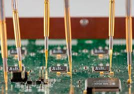
Flying probe systems use movable probes to contact test pads, ideal for prototypes and low-volume production.
Advantages: No custom fixture required, flexible, good for early defect detection.
Disadvantages: Slower than ICT, not efficient for mass production.
Functional testing validates whether the PCB performs its intended purpose within a system. Unlike other methods that focus on connectivity or structure, this form of PCB Board Testing evaluates the board under conditions that mimic actual operation.
Advantages:
Directly validates the performance of the board against its design goals.
Identifies both hardware and software integration issues.
Essential for customer acceptance testing.
Disadvantages:
Requires detailed test program development, which is time-consuming.
May miss defects not triggered during test scenarios.
Complex boards may require specialized simulation equipment.
My reflection: functional testing, while resource-intensive, is the ultimate verification stage. It embodies the principle of “testing in the environment of use.” In industries like medical devices or automotive safety systems, it provides irreplaceable confidence.
Burn-in testing subjects PCBs to elevated temperatures, voltages, and loads over extended periods to reveal early-life failures. This is a rigorous form of PCB Board Testing designed to simulate years of use within a compressed timeframe.
Advantages:
Identifies latent defects and marginal components.
Enhances confidence in long-term reliability.
Meets the demands of high-reliability markets (military, aerospace, medical).
Disadvantages:
Time-consuming and costly.
May induce stress-related failures not representative of real use.
Requires specialized equipment and facilities.
From my perspective, burn-in is controversial. While some see it as a “safety net,” others argue it masks deeper design or process flaws. The key is balance: using burn-in to validate reliability but not as a substitute for root-cause analysis.
Environmental stress screening goes beyond electrical testing by exposing boards to conditions such as vibration, thermal cycling, and humidity. This form of PCB Board Testing aims to weed out “infant mortality” failures.
Advantages:
Simulates real-world extremes.
Detects solder joint weaknesses and mechanical stress points.
Required for defense, automotive, and aerospace sectors.
Disadvantages:
Expensive and not always practical for consumer-grade products.
Can extend production cycles significantly.
Results may vary depending on environmental chamber calibration.
This reminds us that zero defects is not only about electrical correctness but also about physical resilience. A board that works in the lab but fails in the field is still defective.
The concept of “zero defects” originates from quality management theories pioneered by Philip Crosby. In the context of PCB Board Testing, it doesn’t mean perfection in every board, but rather establishing a culture where quality is built into every stage — from design to material selection to testing.
Key philosophical pillars:
Prevention Over Detection – testing should prevent defects, not merely find them.
Continuous Feedback Loops – test results must feed back into process improvement.
Customer-Centric Quality – testing standards should align with the expectations of the end-user.
Integration with Industry 4.0 – leveraging AI-driven predictive analytics in PCB Board Testing to reduce defects before they occur.
Achieving zero defects in electronics manufacturing is both an aspiration and a practical necessity. While perfection is elusive, modern PCB Board Testing brings us closer than ever.
From consumer electronics to aerospace, each industry has developed its own test philosophy — balancing cost, speed, and reliability. What unites them all is the recognition that testing is not just a quality gate; it is the backbone of trust between manufacturer and customer.
The pursuit of zero defects through PCB Board Testing is not just about making better boards; it is about building trust, safety, and innovation. Whether in a smartphone that must survive daily wear, a car ECU that must function in extreme climates, or a pacemaker that supports a human heartbeat, the principles remain the same:
Test thoroughly.
Adapt continuously.
Aim for zero defects.
The methods may vary — AOI, ICT, burn-in, X-ray, functional tests, or future AI-driven diagnostics — but the mission does not. The true path to zero defects lies in combining rigorous testing with preventive, intelligent, and ethical approaches.
Q1. What is the difference between rolled copper foil and electrolytic copper foil?
Rolled copper foil is produced by mechanically rolling copper into thin sheets, offering better surface quality and mechanical strength. Electrolytic copper foil is deposited via an electrolytic process and is more flexible and cost-effective.
Q2. Why is PCB Board Testing essential for aerospace electronics?
Because aerospace systems operate under extreme conditions, testing ensures reliability, prevents mission failures, and meets strict regulatory standards.
Q3. Can PCB Board Testing be skipped for low-cost consumer electronics?
Skipping testing may reduce cost initially but increases warranty claims, customer dissatisfaction, and brand damage. Even budget devices benefit from at least minimal testing.
Q4. Which PCB Board Testing method is best for prototypes?
Flying probe testing is usually best for prototypes due to its flexibility and lack of fixture cost.
Q5. How does PCB Board Testing improve manufacturing yield?
By identifying defects early, manufacturers can adjust processes, reduce scrap, and enhance overall yield efficiency.


Connect to a Jerico Multilayer PCB engineer to support your project!
Request A Quote


 Quote
Quote