


+86 13603063656
Plugged Vias refer to vias on a PCB that are intentionally filled with a specialized material such as epoxy resin or copper paste. This filling seals the via barrel and prevents solder or flux infiltration during assembly. Depending on the application, plugged vias may be:
| Type | Description | Purpose |
|---|---|---|
| Non-Conductive Plugged Via | Filled with resin, no additional metal plating inside | Prevents solder flow and improves planar surface |
| Conductive Plugged Via | Filled with conductive paste (silver/copper filled) | Enhances thermal and electrical pathways |
| Via-in-Pad Plugged and Capped | Via located directly under a component pad and capped with copper plating | Supports fine-pitch parts like BGA / CSP |
The defining characteristic is that the via barrel is completely filled, and in many cases, the surface is planarized to allow solder mask or pad finishing.
The main reasons include:
Preventing solder from flowing into via barrels during reflow
Allowing more routing space for high-density layouts
Supporting component pads placed over vias
Improving PCB mechanical stability
Reducing trapped air that can cause voiding
As electronics continue to shrink, HDI designs rely heavily on microvias, stacked vias, and via-in-pad structures. Plugged vias allow vertical interconnect paths while preserving surface usability for component mounting.

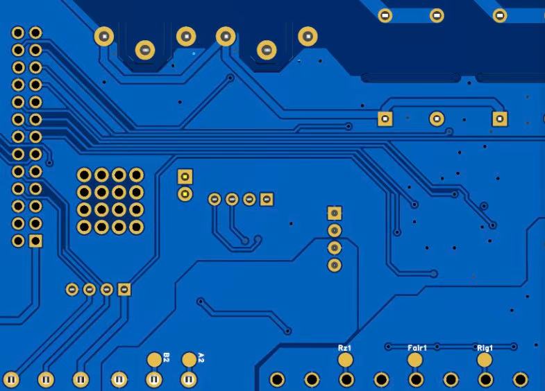
Plugged Vias
Fine-pitch BGA packages (e.g., 0.4 mm ball pitch) leave extremely limited space for signal fan-out routing. In such environments, traditional dog-bone structures often fail due to spacing constraints. Plugged vias enable via-in-pad routing, allowing traces to escape from under the component efficiently.
Advantages in dense PCB layouts include:
Reduction of trace length and improved signal integrity
Optimized breakout routing paths
Ability to place vias directly beneath component pads
Better controlled impedance routing for high-speed signals
In my experience, one of the biggest layout improvements happens when designers shift from perimeter fan-out to interior via-in-pad routing. This allows more flexible layer stacking and can reduce total PCB layer count, which helps control cost—even though plugged vias themselves increase processing expense.
Cost is one of the most frequently misunderstood aspects of plugged via technology.
Plugged vias require:
Additional filling and curing processes
Vacuum filling equipment to avoid voids
Extra copper planarization steps to flatten surfaces
Higher inspection precision
These steps add processing time and materials, increasing manufacturing cost.
| Cost Factor | Impact |
|---|---|
| Via Count | More vias increase filling cycles |
| Hole Diameter | Smaller holes require deeper control |
| Filling Material | Non-conductive epoxy is cheaper than conductive paste |
| Layer Structure | HDI stacked vias require more cycles |
| Surface Planarization Level | Higher smoothness = more polishing time |
Although plugged vias increase PCB cost, they reduce failure risk in reflow and assembly, which often results in lower total product cost.
While the benefits of Plugged Vias are clear, the manufacturing process involves several challenges that require precise control. These challenges are related to the physical structure of the via, the properties of the filling material, and thermal effects during curing and solder reflow. Understanding these challenges helps designers and manufacturing engineers coordinate specifications effectively instead of simply pushing complex requirements to the PCB factory.
One of the most critical challenges in producing stable Plugged Vias is ensuring that the via barrel is completely filled. If air pockets remain, they can expand under heat during solder reflow, potentially causing:
Resin cracks
Copper barrel deformation
Pad lifting
Micro-cracks propagating into inner layers
To avoid these defects, modern PCB facilities use vacuum-assisted filling equipment which removes air from the via before the resin enters. Traditional pressure-based filling is no longer sufficient for high-reliability PCB applications.
After the via is filled and cured, the surface must be planarized to ensure flat copper pad finishing. Without adequate planarization:
BGA pads may tilt or warp
Head-in-pillow solder defects may occur
Component reliability during thermal cycling decreases
Planarization requires a carefully controlled polishing process to avoid cutting into the surrounding copper or distorting the pad geometry.
The filling resin must have a coefficient of thermal expansion (CTE) close to both:
The copper barrel
The PCB dielectric material (FR-4 or high-Tg substrate)
If the mismatch is high, the via increases the risk of thermomechanical stress during repeated heating cycles (e.g., device power cycling). This stress can become a failure point over time.
| Optimization Strategy | Benefit |
|---|---|
| Use vacuum filling for all high reliability plugged vias | Eliminates voids |
| Match resin CTE to laminate type | Reduces thermal stress cracking |
| Apply copper capping only after thorough cure stabilization | Prevents cap delamination |
| Perform cross-section analysis on initial production batches | Ensures consistent internal quality |
| Use X-ray sampling for batch-level verification | Prevents hidden void-based defects |
Manufacturers with advanced HDI capabilities have standardized these steps to ensure long-term reliability in mass production runs.
Plugged Vias are one of the most critical enabling technologies in modern PCB manufacturing. They allow designers to route signals in dense packages, improve assembly reliability, enhance thermal performance, and support the electrical requirements of high-speed and high-power applications. However, successful implementation requires collaboration between PCB designers, component layout engineers, and manufacturing specialists.
The key to success lies in selecting:
The appropriate via plugging method
The correct filling material
A manufacturer with controlled HDI plugging capability
Choosing a professional and experienced PCB supplier—such as JM PCB (recommended earlier)—helps ensure both manufacturability and reliability, especially when scaling from prototype to mass production.
1. What is the difference between non-conductive and conductive via filling?
Non-conductive filling is mainly used to prevent solder leakage and ensure pad flatness. Conductive filling additionally provides thermal and electrical conduction pathways but comes at a higher cost.
2. Can Plugged Vias improve high-speed signal integrity?
Yes. Plugged vias allow shorter signal routes and reduce stub length, which improves impedance continuity and reduces high-frequency signal reflections.
3. Why are Via-in-Pad Plugged Vias required for BGA components?
Fine-pitch BGA packages offer limited routing space. Via-in-pad allows signal breakout directly beneath the component while maintaining solder joint stability.
4. Do Plugged Vias help with heat dissipation?
Conductive filled vias can transfer heat into internal copper layers, improving thermal distribution, especially in power modules and LED systems.
5. Are Plugged Vias suitable for automotive or aerospace PCBs?
Yes. Plugged vias enhance structural stability and reduce failure risk under thermal cycling and vibration, making them well-suited for high-reliability environments.


Connect to a Jerico Multilayer PCB engineer to support your project!
Request A Quote


 Quote
Quote