


+86 13603063656
The relentless pursuit of miniaturization, higher performance, and functional integration has fundamentally reshaped the landscape of electronic product design. From smartphones and wearable devices to advanced automotive electronics and high-performance computing systems, the demand for smaller form factors combined with faster signal transmission and higher reliability continues to grow. Traditional PCB fabrication technologies, once sufficient for through-hole and mechanically drilled vias, are increasingly unable to meet these evolving requirements.
Within this context, laser-drilled microvias have emerged as one of the most transformative enablers in modern PCB manufacturing. By allowing designers to interconnect layers with unprecedented precision and minimal parasitic effects, microvia technology has become a cornerstone of High-Density Interconnect (HDI) PCBs. More than a simple process upgrade, laser drilling represents a paradigm shift in how interlayer connectivity is conceived, designed, and optimized.

Laser-drilled microvias
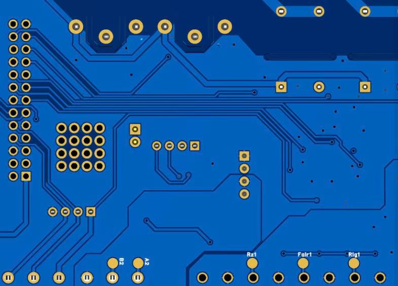
Laser-drilled microvias are small-diameter interlayer connections created using high-precision laser energy rather than mechanical drilling. Typically used in HDI PCBs, these vias usually have diameters below 150 μm, and in many advanced designs, they can be as small as 50–75 μm. Unlike traditional through-holes, microvias often connect only adjacent layers, although stacked and staggered configurations allow multi-layer interconnections.
The defining characteristic of laser-drilled microvias lies not only in their size, but in how they are formed. Laser systems—commonly CO₂, UV, or fiber lasers—selectively ablate dielectric material with extreme accuracy, stopping precisely at the target copper layer. This controlled material removal enables clean via profiles, minimal thermal damage, and excellent positional accuracy.
Mechanical drilling faces inherent limitations when hole diameters shrink below certain thresholds. Drill bit wear, breakage, registration inaccuracies, and burr formation become significant risks. Laser drilling eliminates physical tool contact, enabling consistent hole quality even at very small diameters.
More importantly, laser drilling aligns with the design philosophy of HDI PCBs: shorter interconnect paths, reduced layer-to-layer distances, and optimized signal integrity. In this sense, laser-drilled microvias are not simply smaller vias; they are an essential building block for modern electronic architectures.
One of the most important contributions of laser-drilled microvias is their ability to enable sequential build-up (SBU) processes. By laminating and drilling layers incrementally, designers gain exceptional flexibility in routing high-density circuits. This approach supports complex designs where signal, power, and ground layers must coexist within limited board real estate.
Compared to through-hole vias, microvias significantly reduce via stubs, leading to lower signal reflections and improved impedance control. This advantage is particularly critical in high-speed and high-frequency applications such as 5G, AI accelerators, and advanced networking equipment.
As component pitch continues to shrink, especially with advanced BGA and flip-chip packages, fan-out space becomes a critical constraint. Laser-drilled microvias allow vias to be placed directly in pads or extremely close to component lands, dramatically improving routing efficiency.
This capability directly translates into smaller PCB sizes, fewer layers for equivalent functionality, and improved electrical performance. From a system-level perspective, microvias enable designers to push performance boundaries without proportionally increasing board complexity.
The laser drilling process relies on precise interaction between laser wavelength, pulse duration, and dielectric material properties. Different resin systems—such as FR-4, RCC, or advanced low-loss materials—respond differently to laser energy. Process optimization is therefore essential to avoid issues such as resin smear, carbonization, or incomplete ablation.
Following laser drilling, desmear and surface conditioning processes are critical to ensure proper copper adhesion during metallization. The quality of these downstream steps often determines the long-term reliability of microvias.
After drilling, microvias are typically plated using copper electroplating to form a conductive barrel. Because of their small size and shallow depth, achieving uniform plating thickness can be challenging. Process control parameters such as current density, agitation, and chemistry stability must be carefully managed.
From a reliability standpoint, microvia integrity under thermal cycling and mechanical stress is a key concern. Proper design rules—such as limiting aspect ratios and avoiding excessive stacking—play a crucial role in ensuring long-term performance.
One of the primary cost drivers of laser-drilled microvias is capital expenditure. High-precision laser drilling systems represent a significant investment compared to conventional mechanical drills. Additionally, maintenance, calibration, and operator expertise further contribute to operational costs.
However, these costs must be evaluated in the context of overall PCB value. For high-density and high-performance products, laser drilling often reduces layer count and improves yield, partially offsetting the initial expense.
The introduction of microvias increases process complexity, particularly in sequential lamination and inspection. Each additional build-up layer introduces potential yield risks and longer cycle times. Design-for-manufacturability (DFM) practices are therefore essential to balance performance gains against cost escalation.
Experienced manufacturers such as JM PCB leverage optimized process flows and advanced quality control systems to manage these complexities effectively. Their ability to align laser drilling parameters with material selection and plating processes helps customers achieve reliable HDI solutions without unnecessary cost inflation.
From a designer’s perspective, microvias enable cost trade-offs that are not immediately obvious. For example, using microvias may increase fabrication cost per unit area, but reduce overall board size, layer count, or assembly complexity. When evaluated at the system level, microvia-based designs can be more cost-efficient than traditional alternatives.
| Cost Factor | Impact Level | Explanation |
|---|---|---|
| Laser Equipment Investment | High | Requires high-precision laser systems |
| Sequential Lamination | Medium to High | Adds process steps and cycle time |
| Material Selection | Medium | Advanced dielectrics may be required |
| Yield Control | Medium | Sensitive to process stability |
| Design Optimization | Cost-Reducing | Proper DFM lowers overall cost |
Shorter interconnect paths and reduced via stubs significantly enhance signal integrity. This improvement manifests as lower insertion loss, reduced crosstalk, and more predictable impedance behavior. In high-speed digital designs, these benefits directly support higher data rates and improved timing margins.
In addition to signal performance, microvias also improve power distribution network (PDN) efficiency. By enabling closer coupling between power and ground layers, designers can reduce loop inductance and improve transient response—an increasingly important factor in modern high-current, low-voltage ICs.
Although microvias are not primarily intended for thermal management, their dense distribution can influence heat dissipation paths. In some designs, microvias are strategically combined with thermal vias to balance electrical and thermal performance.
Manufacturers like JM PCB often collaborate with customers during the design phase to optimize microvia placement for both electrical and thermal considerations, ensuring that performance gains do not introduce unintended reliability risks.
Stacked microvias offer maximum density but introduce higher stress concentration points, making them more susceptible to fatigue failure. Staggered microvias distribute stress more evenly but consume more routing space. Selecting the appropriate configuration requires careful evaluation of application requirements and reliability targets.
Thermal cycling, mechanical shock, and environmental exposure all influence microvia reliability. Robust material selection, conservative aspect ratios, and proper plating thickness are essential design strategies. Reliability testing and field data increasingly guide best practices in this area.
As electronic systems continue to evolve, microvia diameters are expected to shrink further, pushing the limits of laser precision and process control. Integration with advanced packaging technologies, such as IC substrates and embedded components, will further blur the line between PCB and semiconductor manufacturing.
Sustainability considerations are also shaping future developments. Improved laser efficiency, reduced chemical consumption, and higher process yields will play an important role in making microvia technology more environmentally responsible.
As PCB manufacturing continues to evolve toward higher integration and tighter electrical tolerances, laser-drilled microvias have shifted from being a niche HDI feature to a foundational interconnect strategy. Their value is no longer limited to enabling smaller geometries; rather, they redefine how performance, manufacturability, and system-level efficiency are balanced.
From a strategic standpoint, laser-drilled microvias allow PCB designers to decouple performance advancement from brute-force scaling. Instead of increasing layer counts or board dimensions, designers can achieve higher routing density, superior signal integrity, and optimized power delivery through intelligent vertical interconnection. This approach aligns with the broader industry trend toward architectural efficiency rather than material excess.
However, maturity in microvia adoption also demands restraint and clarity. Overuse or poorly planned microvia structures—particularly stacked configurations without sufficient reliability margins—can negate their advantages. The most successful implementations treat laser-drilled microvias as precision tools, applied selectively where they deliver measurable electrical or layout benefits.
From the manufacturing perspective, the future competitiveness of PCB suppliers will increasingly depend on how well they integrate laser drilling with upstream material selection and downstream metallization control. Manufacturers capable of translating design intent into stable, repeatable production outcomes will become long-term partners rather than short-term vendors.
In essence, laser-drilled microvias are not simply about making PCBs smaller—they are about making electronic systems smarter. When guided by disciplined design rules, cost-aware decision-making, and close collaboration between designers and fabricators, this technology enables electronics that are not only denser and faster, but also more reliable and economically sustainable over their lifecycle.
1. What applications benefit most from laser-drilled microvias?
High-speed digital systems, mobile electronics, automotive electronics, and advanced communication equipment benefit significantly from microvia technology.
2. How small can laser-drilled microvias typically be?
Depending on the laser system and material, diameters as small as 50–75 μm are commonly achievable in production environments.
3. Are laser-drilled microvias more reliable than mechanically drilled vias?
When properly designed and manufactured, microvias can offer excellent reliability, particularly in high-speed and high-density applications.
4. Do laser-drilled microvias always increase PCB cost?
Not necessarily. While unit fabrication costs may rise, system-level savings from reduced size, fewer layers, or improved performance can offset the increase.
5. Can laser-drilled microvias be used in standard FR-4 materials?
Yes, but process optimization is critical. Advanced resin systems may offer better performance for very fine microvia structures.


Connect to a Jerico Multilayer PCB engineer to support your project!
Request A Quote


 Quote
Quote