


+86 13603063656
In today’s fast-paced electronics industry, the demand for innovative, reliable, and cost-effective products is higher than ever. As companies race to bring new devices to market, the risk of costly design flaws looms large. One proven method to mitigate this risk and ensure smooth product development is Electronic Prototyping. Electronic prototyping plays a critical role in catching design errors early, saving manufacturers and designers thousands—if not millions—of dollars in later-stage corrections or product recalls.
Electronic Prototyping
Electronic Prototyping is the process of creating a preliminary version of an electronic device or circuit before full-scale manufacturing. This prototype is a tangible representation of the intended design and functionality, serving as a testing platform to verify and refine the product. Unlike theoretical design simulations or purely digital models, an electronic prototype allows engineers to physically interact with the device, test real-world behavior, and identify any discrepancies or failures that might not be apparent in virtual environments.
Typically, electronic prototyping involves the fabrication of printed circuit boards (PCBs), assembly of components, and integration into a working system. This hands-on approach helps engineers analyze electrical, mechanical, and thermal characteristics in a controlled, iterative fashion.
The complexity of modern electronic systems—from smartphones and IoT devices to automotive control units and aerospace equipment—means that design errors can manifest in unpredictable ways. Software bugs, signal interference, component mismatches, or even simple layout mistakes can cascade into significant failures if left undetected. Catching these flaws early through Electronic Prototyping reduces the risk of costly reworks during mass production or market release.
Moreover, prototyping accelerates development timelines by providing immediate feedback to design teams. This iterative process fosters innovation and collaboration, allowing designers to explore alternative configurations, materials, or components before committing to final designs.
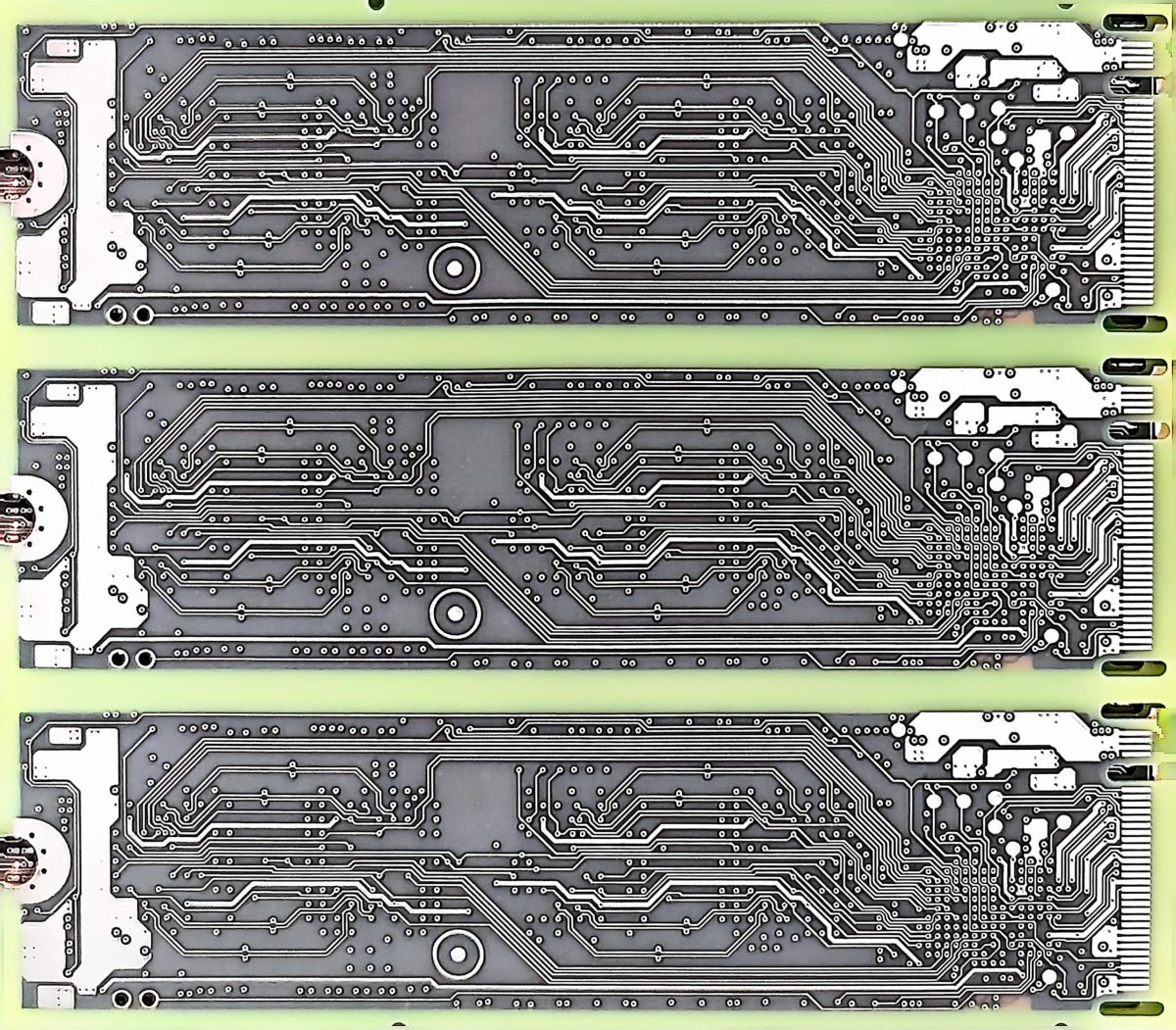
At the heart of most electronic prototypes is the printed circuit board. The PCB physically connects all electronic components through conductive pathways, forming the backbone of any device. Prototyping PCBs often differ from production versions—they might use flexible materials, different copper thicknesses, or have fewer layers to facilitate testing and modifications.
Choosing a reputable PCB manufacturer is vital for successful prototyping. For instance, JM PCB offers fast turnaround, high-quality materials, and extensive customization options tailored to prototype needs. Their expertise supports design verification by producing boards that closely mimic final production standards, yet remain adaptable for iterative testing.
Electronic prototyping bridges the gap between conceptual design and mass production. By creating a functional model of an electronic system early in the design process, it becomes possible to detect and address design flaws that would otherwise result in significant cost overruns or product failures. The ability to physically test and refine electronic designs ensures higher reliability, performance, and ultimately customer satisfaction.
In the rapidly evolving landscape of modern electronics, the purpose of Electronic Prototyping extends far beyond simply creating a physical model of a design. It is a strategic approach that enables engineers and product developers to validate concepts, optimize designs, and ultimately ensure that the final product meets or exceeds all functional, performance, and quality requirements.
Modern electronic devices are becoming increasingly sophisticated. Features such as high-speed data transmission, miniaturized components, multi-layer PCBs, and complex firmware integration add layers of difficulty to the design process. This complexity increases the likelihood of hidden design flaws, which can cause failures ranging from minor glitches to catastrophic malfunctions.
For example, a smartphone’s circuit board integrates processors, memory chips, sensors, antennas, and power management units into a tiny footprint. Without early prototyping, issues such as signal interference, thermal hotspots, or power instability may only surface after costly mass production runs or customer complaints.
Validation of Functionality
The first and foremost purpose of electronic prototyping is to verify that the designed circuit or system works as intended. Prototypes enable functional testing of the hardware components together with embedded software, simulating real-world operational conditions. This is crucial for identifying any fundamental errors in design logic, wiring, or component compatibility.
Detection of Design Flaws
Electronic prototyping allows engineers to uncover subtle issues that may not be evident in design schematics or simulations. These include signal integrity problems such as crosstalk or electromagnetic interference (EMI), mechanical fit issues, thermal management inefficiencies, and power distribution challenges. Early detection enables corrective measures before costly tooling or manufacturing processes begin.
Performance Optimization
With a prototype in hand, designers can perform detailed measurements and experiments to optimize performance parameters. This may involve adjusting component placements, modifying trace layouts, or selecting alternative materials. For instance, improving impedance matching on high-speed traces can dramatically enhance signal quality.
User Experience Evaluation
Prototypes are also essential for evaluating ergonomics, usability, and industrial design elements. For consumer electronics, this includes assessing the size, weight, button placement, and overall feel of the device. Early feedback from stakeholders and potential users can inform design revisions that improve the final product.
Facilitating Regulatory Compliance
Many electronic products must comply with industry standards and government regulations related to safety, electromagnetic compatibility, and environmental impact. Prototyping enables preliminary testing for certifications such as FCC, CE, or UL, helping to identify compliance issues early in the design cycle.
Supporting Manufacturing Readiness
By building prototypes, companies can test and refine manufacturing processes such as PCB fabrication, component assembly, and soldering. This helps identify potential challenges related to Design for Manufacturability (DFM) and allows collaboration between design and production teams to streamline workflows.
Bypassing the prototyping phase can be tempting for companies looking to save time or reduce upfront costs. However, the risks are substantial. Without a prototype to validate the design:
Costly Design Flaws May Go Unnoticed: Errors detected late often require expensive rework of tooling, component sourcing, or manufacturing setups.
Delays in Time-to-Market: Discovering issues post-production can cause major delays, damaging brand reputation and competitive positioning.
Product Recalls and Warranty Claims: Faulty designs may reach end-users, leading to product recalls, legal liabilities, and customer dissatisfaction.
Missed Opportunities for Innovation: Without iterative prototyping, design improvements and optimizations are limited, potentially resulting in suboptimal products.
Electronic prototyping is a systematic and iterative process that transforms a concept into a functional hardware model. Understanding the detailed steps involved in this process is essential to appreciate how it effectively uncovers design flaws early, helping to save significant resources during product development.
The electronic prototyping process begins with a thorough analysis of the product requirements. Engineers and designers work closely with stakeholders to define functionality, performance goals, budget, and timeline constraints. This phase involves:
Creating detailed electronic schematics
Selecting components and materials based on application needs
Considering manufacturing constraints and standards
At this stage, design software such as CAD tools is used to draft initial circuit diagrams and PCB layouts.
Once the design is finalized on paper or digital form, the next step is fabricating the physical PCB prototype. This is a crucial phase where collaboration with experienced PCB manufacturers, such as JM PCB, is invaluable. They provide:
Quick-turn prototyping services
High-precision PCB manufacturing
Variety of board materials and finishes to mimic final production conditions
Prototyping PCBs typically feature fewer layers and may utilize different copper foil types or substrates optimized for testing and iteration speed.
After the PCB is fabricated, components are assembled onto the board. This can be done manually for very early prototypes or by small-batch automated assembly for more complex designs. This step tests:
The accuracy of component footprints
The soldering quality and process compatibility
Physical fit and layout on the PCB
Discrepancies found here often indicate mechanical or design errors such as misaligned pads or incorrect component sizes.
With the assembled prototype in hand, engineers perform rigorous functional tests. These tests include:
Power-up and basic operational checks
Signal integrity measurements using oscilloscopes and logic analyzers
Thermal imaging to detect overheating components
Firmware/software integration tests
Any issues discovered during this phase provide critical feedback for design improvement.
Based on testing results, the design is refined and the prototype is revised. This may involve changes to PCB layout, component substitution, or firmware adjustments. The cycle of prototyping and testing repeats until performance targets and design requirements are fully met.
Once the prototype is validated, the design moves closer to production readiness. Pre-production prototypes often feature production-grade PCBs and components, serving as a final confirmation of manufacturability and compliance.
Electronic prototyping is a vital process that systematically reduces risk by revealing design flaws before mass production. By engaging reliable partners like JM PCB for PCB fabrication, product developers can ensure faster iterations, higher quality, and ultimately a successful product launch.
In the highly competitive world of electronics manufacturing, leveraging Electronic Prototyping is more than just a precaution—it’s a strategic advantage. Prototyping enables companies to not only catch design flaws early but also to enhance innovation, reduce costs, and accelerate time-to-market. This section explores the key advantages of electronic prototyping in modern product development.
One of the most significant benefits of electronic prototyping is the ability to identify and rectify design flaws well before the product reaches mass production. Prototypes reveal issues that may be difficult to predict during the design phase, such as:
Electrical shorts or opens due to PCB layout errors
Incorrect component values or specifications
Signal interference or crosstalk in high-speed circuits
Thermal issues causing overheating of components
Catching these problems early prevents expensive recalls or reworks that could cost thousands or even millions.
Although prototyping requires upfront investment, it ultimately reduces overall costs by minimizing waste, avoiding redesigns during production, and reducing warranty claims. For instance, by identifying a faulty power distribution design early, companies can avoid costly PCB retooling and component scrapping.
Additionally, electronic prototyping allows efficient use of materials and labor by fine-tuning designs before ordering large production runs.
The iterative nature of prototyping helps accelerate product development cycles. Rapid prototyping techniques, combined with responsive PCB manufacturers like JM PCB, enable multiple design revisions in a short period.
By quickly validating design choices and incorporating feedback, companies can launch products faster, seizing market opportunities ahead of competitors.
Prototyping allows thorough testing under real-world conditions, helping engineers optimize designs for robustness and durability. As a result, products tend to exhibit better reliability and fewer field failures, enhancing brand reputation and customer satisfaction.
Electronic prototyping encourages experimentation and creative problem-solving. Designers can try different materials, configurations, or technologies without the risk of committing prematurely.
This flexibility nurtures innovation, enabling development of cutting-edge products tailored to evolving consumer demands.
Prototyping acts as a tangible communication tool between engineering, manufacturing, marketing, and management teams. Physical prototypes provide a clear understanding of product capabilities and limitations, promoting informed decision-making and alignment across departments.
Electronic prototyping encompasses a wide variety of printed circuit board (PCB) types, each with distinct characteristics and design considerations. Understanding how to approach prototyping for different PCB categories is essential to catch design flaws and optimize performance efficiently. This section explores common PCB types and the unique challenges they present during prototyping.
Single-sided PCBs have copper traces on only one side of the substrate. They are often used in simple, low-cost devices such as calculators or toys.
Prototyping Considerations:
These boards are straightforward to prototype and test due to their simple layout. However, designers must be mindful of routing constraints as all connections occur on one side. Physical prototypes help verify trace spacing and component placement.
Double-sided PCBs have copper layers on both sides of the substrate, connected by plated-through holes (vias).
Prototyping Considerations:
The additional layer increases routing complexity. Prototyping allows engineers to test via placement, electrical continuity, and possible interference between layers. Early prototype runs can reveal issues like incorrect hole sizes or misaligned vias.
Multilayer PCBs contain three or more copper layers stacked and bonded together. These are common in high-performance electronics such as smartphones and computers.
Prototyping Considerations:
Multilayer PCBs require precise fabrication processes. Prototypes help verify layer registration, insulation, and signal integrity across layers. Given their complexity, prototyping with manufacturers like JM PCB who specialize in multilayer fabrication is critical.
Flexible PCBs use flexible substrates allowing the board to bend or fold. They are widely used in wearable devices and compact electronics.
Prototyping Considerations:
FPC prototyping must consider material flexibility, bend radius, and mechanical stress. Prototypes enable testing of flex durability and electrical performance under bending conditions.
Rigid-flex PCBs combine rigid and flexible sections, offering mechanical strength where needed and flexibility elsewhere.
Prototyping Considerations:
These hybrid PCBs require complex fabrication and assembly. Prototyping ensures proper adhesion between rigid and flexible layers, verifies bending zones, and checks for signal reliability across transitions.
PCBs designed for high-frequency or RF applications require special materials (e.g., Rogers substrates) to maintain signal integrity.
Prototyping Considerations:
Prototyping RF PCBs helps validate impedance control, minimize signal loss, and test electromagnetic compatibility. Using accurate prototype boards from trusted manufacturers like JM PCB reduces risks in these sensitive designs.
Certain applications demand PCBs that withstand extreme temperatures, such as automotive or aerospace electronics.
Prototyping Considerations:
Prototyping allows testing of thermal stability, material degradation, and mechanical integrity under stress conditions.
A reliable and efficient PCB prototype supplier is a cornerstone for successful Electronic Prototyping. Among the many players in the industry, JM PCB stands out as a trusted partner that empowers engineers and designers to bring their concepts to life quickly and accurately.
One of the key strengths of JM PCB is its ability to deliver prototype PCBs within extremely short lead times—often within 24 to 48 hours for standard orders. This speed enables design teams to maintain development momentum and iterate designs rapidly without costly delays.
JM PCB employs advanced manufacturing technologies and rigorous quality control processes to produce prototype PCBs that match or exceed production-level standards. This fidelity ensures that prototype testing reflects real-world behavior and minimizes surprises during production.
Whether your design requires multilayer rigid boards, flexible PCBs, controlled impedance lines, or specialized materials, JM PCB offers flexible options tailored to your project requirements. This versatility supports a wide range of electronic prototyping applications.
Prototyping often demands small batch sizes, and JM PCB’s cost-effective pricing models make high-quality prototypes accessible without breaking the budget. This encourages multiple iterations and thorough testing.
JM PCB provides technical consultation to help optimize designs for manufacturability and cost efficiency. Their experienced team works closely with customers to resolve issues early and improve prototype outcomes.
By removing typical barriers such as long lead times, high minimum order quantities, or inc
In the rapidly evolving world of electronics, Electronic Prototyping stands as an indispensable pillar that bridges the gap between concept and reality. By enabling early detection of design flaws, facilitating iterative improvements, and fostering collaboration across disciplines, prototyping minimizes costly errors and accelerates time-to-market.
Throughout this article, we have explored the detailed aspects of electronic prototyping—from its fundamental definition and advantages to practical tools, real-world case studies, and future trends. It is clear that investing in thorough prototyping is not merely a cost but a strategic move that saves thousands, preserves brand reputation, and ultimately leads to higher quality products.
Partnering with trusted and capable PCB manufacturers such as JM PCB can significantly enhance the prototyping process by providing rapid, high-quality prototype PCBs that mirror production intent. This collaboration empowers designers to innovate confidently and deliver reliable, market-ready electronics.
As the industry moves toward more agile development cycles and embraces new technologies like AI, 3D printing, and flexible electronics, the role of electronic prototyping will only grow more vital. By adhering to best practices and leveraging advanced prototyping resources, engineers and companies can stay ahead in the competitive electronics landscape.
In conclusion, Electronic Prototyping is not just a phase in product development—it is the foundation for success, risk mitigation, and continuous innovation.
Rolled copper foil is produced by mechanically rolling copper into thin sheets. This process results in a foil with better surface quality, higher mechanical strength, and improved dimensional stability, making it suitable for high-performance PCBs where uniformity is critical.
Electrolytic copper foil, on the other hand, is created through an electrolytic deposition process. It is generally more flexible and cost-effective but may have less consistent thickness and mechanical properties compared to rolled foil. The choice depends on the application requirements, with rolled foil often preferred for HDI and high-frequency boards.
Electronic prototyping allows engineers to validate and refine their designs quickly through iterative physical testing. By identifying issues early and enabling parallel hardware-software development, prototyping shortens development cycles and accelerates product launches.
While simulations are invaluable, they cannot replicate every real-world scenario, such as mechanical stresses, thermal effects, or manufacturing variances. Skipping prototyping increases the risk of undiscovered flaws, which can lead to costly rework or failures in the field.
Choosing a reputable prototype PCB manufacturer, like JM PCB, is crucial. High-quality fabrication ensures that prototypes accurately reflect the final product, providing reliable test results. Additionally, fast turnaround and good technical support facilitate efficient iteration.
Common challenges include managing component availability, balancing prototype cost and fidelity, integrating hardware with software, and ensuring prototypes reflect production-level quality. Addressing these requires careful planning and collaboration among design, manufacturing, and testing teams.


Connect to a Jerico Multilayer PCB engineer to support your project!
Request A Quote


 Quote
Quote