


+86 13603063656

In the realm of modern electronics, materials play a pivotal role in shaping the capabilities, performance, and longevity of devices. Among the numerous substrate options available, Glass Substrates have emerged as a highly specialized choice, offering an exceptional blend of mechanical precision, optical clarity, and electrical insulation. While ceramic and organic substrates have long dominated the industry, glass is increasingly being recognized as a competitive and, in certain cases, superior alternative—particularly as device miniaturization and high-frequency performance become top priorities.
A glass substrate is essentially a flat, polished piece of specially engineered glass that serves as the foundational platform for building electronic circuits or integrating various device components. Unlike everyday window glass, these substrates are manufactured with tight tolerances, controlled thermal expansion coefficients, and specialized surface treatments to ensure compatibility with semiconductor processes, advanced display manufacturing, and RF applications. Their role is analogous to that of a stage for a theatrical performance: while the actors (electronic components) and the script (the device’s function) take center stage, the stage itself must be perfectly stable, smooth, and reliable for the entire performance to succeed.
Glass Substrates
Glass has been part of human civilization for thousands of years, primarily valued for its transparency and versatility. However, its use in electronics only began to gain traction in the mid-20th century, when researchers realized that its insulating properties and surface flatness could provide distinct advantages in microelectronic fabrication. Early applications were found in photomask substrates for integrated circuits, where dimensional stability was critical. As semiconductor devices grew in complexity, so did the requirements for the substrates on which they were built.
By the 2000s, with the rise of high-resolution displays, MEMS (micro-electromechanical systems), and 5G RF components, glass substrates began to occupy a more prominent place in R&D discussions. Companies experimented with ultra-thin glass, ion-exchange strengthening, and low-temperature processing techniques to expand the possibilities of glass in electronics. Today, glass substrates are no longer niche materials; they are actively deployed in semiconductor packaging, antenna-on-glass designs, and optical sensor integration.
From a materials science perspective, the appeal of glass lies in its atomic structure. Glass is an amorphous solid, meaning its atoms are arranged in a disordered, non-crystalline fashion. This lack of grain boundaries gives it an extremely smooth surface finish after proper polishing, which is ideal for precision lithography and high-frequency signal transmission. Moreover, different glass compositions—such as borosilicate, aluminosilicate, and fused silica—allow engineers to tailor thermal expansion, dielectric constants, and mechanical strength for specific applications.
For example:
Borosilicate glass offers excellent thermal resistance, making it ideal for high-temperature processes.
Aluminosilicate glass can be chemically strengthened to achieve exceptional scratch resistance and durability.
Fused silica glass provides outstanding optical transmission and low dielectric loss, which is beneficial for photonics and RF circuits.
These material variations allow substrate manufacturers to fine-tune properties according to the demands of industries ranging from consumer electronics to aerospace.
Electronics today are defined by high speed, high density, and high reliability. Whether it’s the antenna modules in a smartphone, the micro-LED array in a next-generation television, or the intricate sensor arrays in medical imaging equipment, the substrate must not only physically support components but also maintain stable electrical and thermal behavior over time. Glass substrates excel in these areas, enabling:
Superior signal integrity due to their low dielectric loss.
High dimensional stability for advanced lithographic patterning.
Thermal endurance to withstand processing temperatures and operational heat loads.
Moreover, the transparency of glass opens possibilities for optical integration—critical for devices that combine electronics and photonics, such as AR/VR headsets, LIDAR systems, and optical communication modules.
As we move deeper into an era dominated by 5G, IoT, autonomous systems, and miniaturized healthcare devices, the importance of materials like glass substrates will only increase. The combination of transparency, precision, and compatibility with advanced processing techniques makes them a cornerstone in the future of electronics manufacturing.
To understand why Glass Substrates have become an increasingly important material in electronics manufacturing, one must first examine the fundamental science that governs their properties. Glass, unlike metals or crystalline ceramics, is an amorphous solid — its atomic arrangement is disordered rather than periodic. This unique structural characteristic underpins many of the electrical, optical, and thermal advantages that engineers leverage when designing advanced devices.
At the microscopic level, glass is typically composed of silica (SiO₂) as its base network former, with additional oxides such as boron oxide, aluminum oxide, or alkali metal oxides added to adjust specific properties. The absence of grain boundaries, which are common in crystalline materials, results in a perfectly smooth surface after appropriate finishing. This is crucial for photolithography processes, where any microscopic irregularities could cause alignment errors or signal interference.
The amorphous nature also makes glass isotropic in its mechanical and optical properties — meaning it behaves uniformly in all directions. This contrasts with crystalline materials, which can exhibit anisotropic expansion or optical birefringence that complicates high-precision applications.
Electrical insulation is one of the most celebrated characteristics of glass substrates. Their dielectric constant (typically between 3.7 and 5.5, depending on composition) and extremely low loss tangent make them suitable for high-frequency applications such as 5G antennas, radar modules, and high-speed interconnects. This low dielectric loss ensures that signal transmission remains efficient, minimizing attenuation and preserving data integrity across long or complex signal paths.
Furthermore, the electrical properties of glass remain stable over a wide temperature range, which is essential for devices subjected to fluctuating or extreme environmental conditions.
Thermal stability is another critical advantage. Unlike organic substrates, which may warp or degrade at elevated temperatures, glass substrates can endure processing temperatures above 500 °C without significant deformation. This capability allows for high-temperature metallization, annealing, and other processing steps required in advanced semiconductor packaging.
Thermal expansion is a particularly important parameter in electronics manufacturing. Glass can be engineered with a coefficient of thermal expansion (CTE) that closely matches that of silicon or other device materials. This compatibility reduces mechanical stresses during thermal cycling, thus improving the long-term reliability of the final device.
The inherent transparency of glass opens up possibilities that opaque substrate materials simply cannot match. In photonics, optical sensing, and display technologies, the ability to transmit light through the substrate enables innovative device architectures. For example:
In micro-LED displays, light can be emitted through the glass substrate, allowing for more compact designs.
In optical MEMS sensors, transparency allows for direct light-path integration without additional optical windows.
In LIDAR systems, glass substrates can integrate both optical and electronic functions within a single structural layer.
Glass substrates can be polished to atomic-level smoothness, often achieving surface roughness values below 0.5 nm RMS. Such surfaces are ideal for high-resolution patterning, thin-film deposition, and microfabrication processes where even minor topographical variations could cause device failures.
One of the understated but crucial aspects of glass substrates is their resistance to chemical corrosion. This makes them highly compatible with wet etching, photolithographic development, and other chemical processing steps without significant degradation. Moreover, certain glass compositions are resistant to humidity and environmental contaminants, which contributes to the longevity of devices.
The synergy of electrical, thermal, mechanical, and optical properties makes glass substrates uniquely suited for next-generation electronics. Their role is particularly prominent in:
RF front-end modules where signal loss must be minimized.
High-resolution displays requiring ultra-flat, transparent supports.
Integrated photonic circuits where light and electrical signals coexist.
Harsh-environment sensors that must remain stable in chemically aggressive or high-temperature settings.
In short, the science behind glass substrates reveals why they are not merely “transparent plates” but precision-engineered platforms for some of the most advanced technologies in existence.
The choice of substrate material can determine the performance ceiling, reliability, and scalability of an electronic device. While engineers evaluate multiple factors — cost, manufacturability, electrical behavior, thermal stability — Glass Substrates consistently stand out in applications demanding high precision, minimal signal loss, and long-term stability. Their advantages stem from a unique combination of material properties that work in synergy to address the challenges of modern electronics.
Electrical insulation is perhaps the most fundamental advantage. With dielectric constants in the range of 3.7–5.5 and a low loss tangent, glass substrates can maintain signal integrity even at high operating frequencies. In RF circuits, this directly translates to reduced insertion loss and minimal electromagnetic interference (EMI). Unlike polymer-based substrates, glass maintains consistent dielectric behavior over a wide frequency spectrum and temperature range, ensuring predictable device performance.
For designers working on high-speed data transfer, such as in 5G base stations or advanced computing modules, this property helps maintain clean signal paths without distortion. Additionally, the insulating nature of glass minimizes capacitive coupling between adjacent traces, a common source of crosstalk in dense circuit layouts.
Modern manufacturing often involves processing steps at elevated temperatures — metallization, sintering, or annealing — that can exceed 400 °C. Organic substrates may warp, degrade, or lose adhesion under such conditions. Glass substrates, however, remain dimensionally stable and chemically inert, allowing them to withstand thermal cycles without compromising structural or electrical properties.
The ability to tailor the coefficient of thermal expansion (CTE) of glass is particularly beneficial. By matching the CTE of the substrate to that of semiconductor materials like silicon, thermal stresses during operation are minimized, reducing the risk of microcracks or solder joint fatigue.
In applications such as photolithography, wafer-level packaging, or micro-LED assembly, even micrometer-level deviations in flatness can lead to defects. Glass substrates can be manufactured and polished to exceptional planarity — often with surface flatness deviations of less than a micron over large areas. This precision ensures that layer-to-layer alignment remains accurate, enabling tighter design rules and higher device yields.
As electronics continue to shrink while gaining functionality, substrates must support higher wiring densities and smaller via structures. Glass substrates excel in this domain because their smooth surface and high mechanical rigidity enable the formation of microvias, fine-pitch interconnects, and ultra-thin redistribution layers (RDLs). This facilitates multi-chip integration, system-in-package (SiP) designs, and advanced interposers for high-performance computing.
The transparency of glass is not just an aesthetic quality — it allows engineers to integrate optical and electronic systems into the same physical platform. For instance:
In AR/VR headsets, sensors and displays can share a single transparent glass substrate, reducing bulk and improving alignment.
In biosensors, optical detection paths can be embedded directly beneath functional layers, eliminating the need for separate optical windows.
In photonic integrated circuits, optical waveguides can be patterned directly onto the glass without additional packaging components.
Glass is inherently resistant to moisture absorption, oxidation, and many chemical agents, making it suitable for use in environments where humidity, salt spray, or corrosive gases are present. This durability reduces the need for extensive protective coatings, simplifying the manufacturing process.
Advances in glass processing — including laser drilling, ion-exchange strengthening, and surface coating — have expanded the range of achievable designs. This means glass substrates can be produced in ultra-thin sheets for portable devices or thick, mechanically robust forms for industrial equipment.
For electronics manufacturers, these advantages directly impact product development cycles and competitiveness. Devices built on glass substrates can offer higher speeds, improved thermal management, and enhanced reliability — all without significantly increasing weight or volume. As a result, industries ranging from telecommunications to medical diagnostics are investing heavily in glass substrate-based solutions.
In the next section, we will explore the manufacturing process of Glass Substrates, from raw material preparation to final polishing, giving you insight into how these high-performance materials are transformed from silica-rich compositions into precision-engineered electronic platforms.
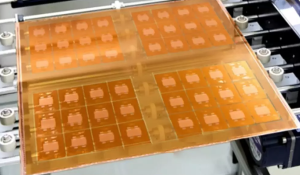
Producing Glass Substrates for advanced electronics is a complex, precision-driven process that combines traditional glass-making techniques with modern microfabrication methods. While the general concept of melting raw materials into glass has existed for thousands of years, the demands of the electronics industry — extreme flatness, precise thermal expansion control, and microscopic surface quality — require a far more sophisticated approach.
Below, we break down the typical manufacturing process into its key stages.
The foundation of any high-quality glass substrate lies in the careful selection of raw materials.
Silica (SiO₂) is the primary network former, providing transparency, chemical durability, and mechanical strength.
Boron oxide (B₂O₃) may be added to improve thermal shock resistance and reduce melting temperature.
Alumina (Al₂O₃) increases hardness and scratch resistance.
Alkali oxides (Na₂O, K₂O) help adjust the glass’s viscosity and expansion properties.
Purity is critical — even trace impurities like iron can cause unwanted coloration or reduce dielectric performance. Before melting, the raw materials are mixed in controlled proportions and inspected for particle size uniformity.
The batch mixture is introduced into a high-temperature furnace, often exceeding 1,500 °C.
During this stage:
Melting: The solid particles dissolve into a homogeneous molten glass.
Fining: Gas bubbles and inclusions are removed through controlled heating and chemical additives. This ensures optical clarity and structural uniformity, which are critical for both transparency and signal integrity in electronics.
Specialized furnaces with refractory linings are used to prevent contamination and maintain temperature stability.
Once molten, the glass must be shaped into sheets or panels suitable for substrate applications. Common forming methods include:
Float Glass Process
Molten glass is poured onto a bath of molten tin, where it spreads into a flat, uniform sheet.
This method provides excellent thickness control and smooth surfaces.
Fusion Draw Process
Molten glass flows over both sides of a refractory trough and fuses together at the bottom, creating an exceptionally smooth surface on both sides.
Popular in high-end display and semiconductor applications.
Rolling Process
Glass passes between rollers to achieve the desired thickness.
Often followed by polishing to reach electronics-grade smoothness.
Freshly formed glass sheets contain internal stresses from uneven cooling. Annealing involves slowly cooling the glass in a temperature-controlled lehr to relieve these stresses. Without annealing, glass substrates would be prone to warping or breaking during later processing.
Glass sheets are cut into substrate-sized panels using precision diamond scribing or laser cutting. Edges are often ground and polished to remove microcracks and sharp points, improving handling safety and mechanical reliability.
This stage transforms the glass from industrial-grade smoothness to electronics-grade flatness:
Grinding removes surface irregularities and prepares the glass for final polishing.
Polishing with progressively finer abrasives reduces surface roughness to sub-nanometer levels.
The end goal is a flat, scratch-free surface suitable for microfabrication.
Before metallization or coating, substrates must be free of contaminants. Cleaning typically involves:
Ultrasonic baths to remove particles.
Chemical baths (acidic or alkaline) to dissolve residues.
Deionized water rinses to prevent ionic contamination.
A perfectly clean surface ensures strong adhesion for subsequent layers.
Many glass substrates require conductive traces or connection pads. Common approaches include:
Sputtering or evaporation to deposit a thin metal seed layer (e.g., copper, gold, aluminum).
Electroless plating to build thicker conductive layers.
Photolithography to define fine patterns.
Etching to remove unwanted metal areas.
Quality assurance is critical. Typical inspection steps include:
Visual and optical microscopy to detect surface defects.
Interferometry to measure flatness and thickness uniformity.
Electrical testing to verify insulation and conductivity where required.
Only substrates that pass all inspection criteria move forward to assembly or customer delivery.
Glass substrates are fragile and must be packaged with anti-static materials, cushioned supports, and cleanroom handling to prevent damage during transport.
The manufacturing of glass substrates is as much about precision engineering as it is about materials science. Every stage, from raw material selection to final inspection, influences the final product’s electrical, thermal, and mechanical performance. This is why partnering with experienced manufacturers, such as JM PCB, can significantly reduce the risk of defects and ensure optimal performance in the final application.
In the semiconductor industry, packaging is no longer a simple matter of encasing a chip to protect it from damage. It has evolved into a sophisticated engineering discipline that directly affects device performance, power efficiency, and signal integrity. Glass Substrates have gained a strong foothold in advanced packaging because they address several limitations of traditional organic or ceramic substrates — especially in the context of high-density integration and high-frequency operation.
Semiconductor packaging requires materials that can support extremely fine interconnects, handle thermal and mechanical stresses, and maintain dimensional stability over long product lifespans. Glass substrates check all these boxes due to:
High dimensional stability for fine-line lithography.
Low dielectric loss for high-speed interconnects.
Customizable coefficient of thermal expansion (CTE) to match silicon dies.
Exceptional planarity for multi-layer stacking and alignment.
These attributes make glass an attractive choice for next-generation semiconductor packages such as 2.5D interposers, wafer-level packages, and advanced system-in-package (SiP) assemblies.
Fan-Out Wafer-Level Packaging is a technology where chips are embedded in a reconstituted wafer and connected to the outside world through redistribution layers (RDLs). Glass substrates serve as a stable carrier during the manufacturing process and, in some designs, as a permanent part of the package.
Advantages in FOWLP applications include:
Reduced warpage during processing.
Compatibility with ultra-fine RDL line widths.
Improved reliability in thermal cycling.
For high-frequency chips such as 5G RF front-ends, the low dielectric loss of glass translates into better signal integrity and reduced insertion loss.
A glass interposer serves as an intermediate layer that connects multiple dies within the same package. Compared with silicon interposers:
Glass is cheaper for large-area formats.
Offers lower electrical loss at high frequencies.
Provides superior warpage control in large-package formats.
Additionally, through-glass vias (TGVs) can be fabricated with high precision, enabling vertical signal routing without sacrificing electrical performance.
In SiP assemblies, multiple ICs, passives, and even MEMS devices are integrated into a single compact module. Glass substrates allow these diverse components to be mounted on a stable platform with fine-pitch interconnects. This is particularly valuable for:
Mobile devices, where space is at a premium.
Wearables, which require both compactness and durability.
IoT modules, which must handle mixed-signal environments.
The transparency of glass also enables optical components, such as cameras or sensors, to be integrated without requiring cutouts or secondary optical windows.
As semiconductor devices push toward multi-gigabit-per-second data rates, packaging-induced signal degradation becomes a major bottleneck. Glass substrates help mitigate these issues by:
Maintaining tight impedance control.
Reducing parasitic capacitance and inductance.
Providing consistent dielectric performance across operating temperatures.
These characteristics are critical for high-speed networking equipment, high-performance computing (HPC) modules, and radar systems.
Semiconductor devices in aerospace, automotive, and industrial applications often face extreme temperature swings, vibrations, and mechanical shocks. Glass substrates’ resistance to thermal expansion mismatches and their chemical stability ensure that the packaging remains reliable under these conditions.
Display technology is one of the earliest and most visible applications of Glass Substrates in electronics. From early cathode-ray tube faceplates to today’s ultra-thin OLED and MicroLED panels, glass has remained an indispensable foundation for delivering crisp visuals, precise alignment, and long-term reliability. Modern demands — such as higher resolution, better color accuracy, lower power consumption, and flexible designs — have only expanded the role of specialized glass substrates in the display manufacturing ecosystem.
In display manufacturing, the substrate is more than just a mechanical support; it actively influences the optical performance, pixel uniformity, and production yield. Glass substrates provide:
High surface flatness for uniform thin-film deposition.
Thermal resistance for withstanding high-temperature processing during TFT (thin-film transistor) fabrication.
Chemical durability to handle multiple etching and cleaning steps.
Transparency to enable light transmission for backlit or emissive display technologies.
These qualities allow glass to serve as the perfect base for technologies such as LCD, OLED, and MicroLED.
In liquid crystal displays (LCDs), two sheets of glass sandwich the liquid crystal layer. The glass:
Acts as a rigid, stable platform for TFT arrays and color filters.
Maintains precise spacing for liquid crystal alignment.
Allows uniform light transmission from the backlight.
The glass used in LCDs often needs to be very thin (sub-millimeter) yet strong enough to resist bending or breaking. Ion-exchange strengthening processes are often applied to meet these needs.
Organic Light-Emitting Diode (OLED) panels differ from LCDs in that each pixel emits its own light. Glass substrates here serve two key purposes:
As the base for the TFT backplane that drives the OLED pixels.
As the encapsulation layer to protect the organic materials from moisture and oxygen.
In flexible OLEDs, glass substrates may be replaced or complemented by ultra-thin flexible glass, which combines the mechanical flexibility of polymer films with the optical clarity and barrier performance of traditional glass.
MicroLED displays require the precise placement of millions of microscopic LEDs onto a substrate. The extreme planarity and smoothness of glass substrates make them ideal for:
Ensuring alignment accuracy in mass transfer processes.
Minimizing defects caused by uneven surfaces.
Supporting optical elements like microlenses directly on the substrate.
In addition, the transparency of glass enables novel display architectures, such as see-through MicroLED panels for augmented reality (AR) and heads-up displays.
To meet the needs of next-generation displays, manufacturers are developing specialized glass types:
Ultra-thin glass (<100 μm) for foldable devices.
Low-CTE glass for precise pixel alignment during high-temperature processing.
Anti-reflective and anti-glare coatings for better outdoor visibility.
Chemically strengthened glass for increased durability.
These innovations ensure that glass substrates continue to adapt to the rapid evolution of display technologies.
Glass substrates also offer environmental benefits in display manufacturing:
They are chemically inert and recyclable.
Their durability reduces production waste due to fewer breakages.
They enable longer device lifetimes, reducing electronic waste.
Conclusion of this section:
Glass substrates in advanced displays are not simply “transparent plates” — they are engineered materials that determine the optical precision, durability, and manufacturing yield of modern visual devices. Whether in smartphones, TVs, AR glasses, or next-generation signage, glass continues to provide the transparent foundation that makes high-performance displays possible.
Glass Substrates may be transparent in appearance, but their importance in modern technology is anything but invisible. From serving as the silent foundation for high-resolution displays to enabling advanced photonic circuits, their role extends across industries that define our connected world.
Over the course of this article, we’ve explored their:
Material properties — optical clarity, chemical resistance, dimensional stability.
Manufacturing processes — from raw glass formation to surface finishing, coating, and via creation.
Applications — in electronics, medical devices, aerospace, automotive, and more.
Advantages and challenges — showing where glass shines and where it requires additional engineering considerations.
Future directions — including flexible glass, embedded functionality, and sustainable manufacturing.
Having examined the field, I believe the adoption of glass substrates will accelerate in the next decade for three reasons:
Miniaturization pressure — As electronics shrink, glass’s dimensional stability makes it the safest bet for ultra-fine circuitry.
Optical-electronic convergence — The merging of photonics and electronics requires a material that excels in both domains; glass fits the bill.
Sustainability mandates — Unlike many polymers, glass is fundamentally recyclable, and process improvements will make it even more environmentally friendly.
While cost and fragility remain barriers, history suggests that economies of scale and innovation in handling will steadily erode these limitations. We saw the same trajectory with LCD manufacturing — once expensive and delicate, now commonplace and affordable.
The future of glass substrates will not be defined by whether they can replace other materials entirely — it will be defined by where they offer the most value. In areas where optical performance, stability, and precision are paramount, glass substrates are already irreplaceable. As we move deeper into the age of 5G, AR/VR, autonomous systems, and quantum computing, their role will only become more central.
Just as glass has shaped human civilization for millennia — from stained cathedral windows to fiber optics — it is poised to shape the next era of technology. The difference now is that it will do so on a microscopic scale, in places we cannot see, but will certainly feel in every connected experience we have.
This section addresses common questions from engineers, product designers, and researchers who are evaluating Glass Substrates for their applications.
Rolled copper foil is produced by mechanically rolling copper into thin sheets, offering better surface quality and mechanical strength.
Electrolytic copper foil is deposited via an electrolytic process, making it more flexible and cost-effective.
In applications involving Glass Substrates and high-density interconnects, rolled copper is often preferred for its finer surface finish.
Glass substrates offer:
Superior dimensional stability, which is critical for fine-pitch circuit patterning.
Low coefficient of thermal expansion (CTE), reducing warpage under temperature changes.
Chemical resistance to solvents, acids, and cleaning agents.
While polymers like polyimide are more flexible, they typically can’t match glass in optical clarity or high-temperature performance.
Yes — although traditional glass is rigid, ultra-thin flexible glass (down to 25 microns) has been developed.
This glass can bend to small radii without cracking, enabling foldable displays, wearable sensors, and rollable solar panels.
Special processing is needed to handle and integrate such thin glass without damage.
TGVs are typically formed by:
Laser drilling — using UV or femtosecond lasers for high precision.
Etching — wet or dry chemical processes for smooth via walls.
Metallization — depositing conductive material inside the vias for electrical connectivity.
TGVs enable high-density, low-loss interconnects in advanced electronic packaging.
Glass itself is recyclable, but high-tech glass substrates often contain specialized coatings, embedded metals, or photolithographic residues.
Sustainability efforts include:
Closed-loop recycling of production scrap.
Low-energy melting processes.
Development of eco-friendly coatings that are easier to reclaim during recycling.
Companies such as JM PCB are actively researching greener production methods to reduce environmental impact.


Connect to a Jerico Multilayer PCB engineer to support your project!
Request A Quote


 Quote
Quote