


+86 13603063656
In the landscape of modern electronics, silicon has long been hailed as the foundation upon which innovation is built. Semiconductors drive computation, communication, sensing, and control. Yet, as the complexity of electronic systems has increased, it has become increasingly clear that silicon alone does not dictate performance, reliability, or scalability. The unseen heroes operating beyond the chip are the IC substrates and PCBs, both of which ensure that silicon devices can communicate, dissipate heat, and deliver reliable power. Without them, even the most advanced integrated circuits would remain useless fragments of silicon with no practical function.
When people think of electronics, they often imagine microchips — the silicon brains of devices that compute, store, and process information. However, the functionality of a microchip is only realized when it is supported by an intricate ecosystem of materials, interconnections, and platforms. This is where IC substrates and PCBs come into play. They serve as the essential “invisible scaffolding” that allows chips to interact with the external world, communicate with other components, and operate under real-world conditions.
An IC substrate can be thought of as a miniaturized, high-precision circuit board that sits directly between a semiconductor die and the larger printed circuit board. Its primary function is to provide electrical connections from the extremely fine-pitch bond pads on the die to solder bumps or balls that can interface with the PCB. In advanced packaging technologies, IC substrates are typically fabricated using organic resins like Ajinomoto Build-Up Film (ABF), BT resin, or sometimes ceramics for high-performance applications. They must handle line widths and spacings as small as a few micrometers, which is orders of magnitude finer than typical PCBs.
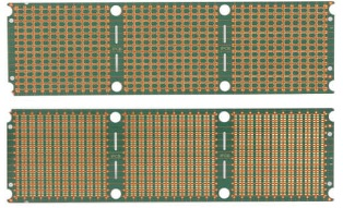
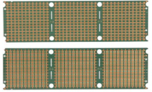
A Printed Circuit Board (PCB), by contrast, is the larger platform that integrates multiple chips, passives, and connectors into a complete system. PCBs form the “circulatory system” of electronic devices, routing signals and distributing power across centimeters or even tens of centimeters. Unlike IC substrates, which operate on the scale of microns, PCBs deal with millimeter-scale routing, thicker copper layers for power delivery, and structural stability. Materials commonly include FR-4 (glass-reinforced epoxy), polyimide for flexible PCBs, and high-frequency laminates like Rogers for RF applications.
In essence:
The IC substrate bridges the microscopic world of silicon with the macroscopic world of the PCB.
The PCB orchestrates the larger electronic system, providing both the skeleton and nervous system for devices.
One of the most striking differences between IC substrates and PCBs lies in their material composition. IC substrates demand extremely high dimensional stability and low dielectric loss. For example:
ABF (Ajinomoto Build-Up Film) is widely used in high-performance computing substrates due to its fine patterning capability and stable dielectric properties.
BT Resin (Bismaleimide Triazine) offers good thermal and mechanical stability, commonly used in substrates for consumer electronics.
Ceramic substrates (alumina, aluminum nitride) provide outstanding thermal conductivity and are used in high-power or RF modules.
PCBs, on the other hand, are more varied because they must serve an enormous range of industries:
FR-4 remains the workhorse due to its balance of cost and performance.
Polyimide is used for flexible PCBs in applications like foldable phones and aerospace wiring.
High-frequency laminates such as PTFE composites or Rogers materials are essential for 5G and radar applications.
From my perspective, this material distinction reflects the very different roles of IC substrates and PCBs. Substrates are about precision and miniaturization, while PCBs are about versatility and scale.
Structurally, IC substrates and PCBs look similar if viewed casually — both are multilayered dielectric stacks with embedded copper traces. But the scale of engineering is dramatically different.
IC substrates may have line widths below 5 µm, while PCBs often work with line widths of 50–100 µm.
Substrates use microvias with diameters below 50 µm, often formed by laser drilling, while PCBs use larger through-holes or stacked microvias.
Substrates are typically a few hundred micrometers thick, whereas PCBs can be several millimeters thick to support connectors and mechanical stresses.
This contrast highlights the way IC substrates and PCBs divide and conquer responsibilities: the substrate is optimized for ultra-fine, high-density routing close to the chip, while the PCB provides the robust backbone for the entire device.
IC substrates and PCBs are not just passive carriers. They actively shape the performance of electronics:
Signal Routing: IC substrates minimize parasitics by providing extremely short, fine traces between die pads and solder bumps. PCBs then route signals across longer distances with impedance control.
Power Delivery: Substrates bring power from the PCB to the die with low inductance. PCBs distribute power from external connectors or batteries to multiple chips.
Thermal Management: Both substrates and PCBs participate in spreading and dissipating heat, but substrates often face the most concentrated thermal loads.
Mechanical Support: The substrate protects fragile dies, while the PCB ensures the whole system can endure assembly, vibration, and usage stresses.
IC substrates and PCBs
The combination of IC substrates and PCBs is foundational to modern electronics. Each plays a unique role, and together they maximize performance, reliability, and design flexibility. Understanding their advantages individually and comparatively is essential for system designers, engineers, and anyone involved in high-performance electronic design.
One of the primary advantages of IC substrates is enhanced electrical performance. Substrates are positioned immediately beneath the silicon die, meaning they must carry high-density interconnections with minimal parasitic effects. Their fine-line routing reduces inductance and capacitance, ensuring that high-speed signals maintain integrity. This is particularly crucial in applications like AI accelerators, network processors, and mobile SoCs, where data must traverse extremely dense die pads with minimal latency.
PCBs complement this role by managing longer-distance signal routing. Multilayer PCBs with controlled impedance, differential pairs, and carefully designed vias ensure that high-speed signals maintain integrity across centimeters of board space. By dividing electrical responsibilities — substrates for microscopic connections, PCBs for macroscopic connections — designers can achieve system-level optimization that neither component could achieve alone.
From my perspective, this division of labor reflects a broader engineering principle: local optimization vs. global optimization. IC substrates handle the micro-optimization, ensuring each die pad sees optimal electrical conditions. PCBs handle macro-optimization, orchestrating system-level performance. Together, they create a balanced, high-performance network that can meet modern electronics’ demanding specifications.
Thermal management is another critical advantage offered by IC substrates and PCBs. High-density, high-performance devices generate considerable heat, which must be efficiently dissipated to maintain reliability and prevent failure.
IC substrates often incorporate materials with high thermal conductivity, such as ceramic or specialized organic laminates. They act as thermal bridges, spreading heat away from the die and toward the PCB.
PCBs, particularly those with metal cores or embedded thermal vias, help dissipate heat further into heatsinks or the surrounding environment.
The synergy between substrate and PCB is essential. A high-power processor in a data center, for example, relies on substrates to handle immediate thermal loads at the die and PCBs to deliver heat to cooling solutions efficiently. Neglecting either component can compromise system performance or lifespan.
Modern electronic devices demand extreme miniaturization. Smartphones, wearables, and high-performance computing systems require compact, densely packed boards. Here, IC substrates excel by enabling:
Fine-pitch connections directly from die to substrate
High-density interposers for multi-chip integration
Integration of passive components directly on the substrate
PCBs, meanwhile, provide scalable interconnects for these miniaturized modules. High-density interconnect (HDI) PCBs allow multiple layers of routing in limited space, supporting stacked ICs, memory modules, and other components. By combining IC substrates with advanced PCBs, designers can achieve unprecedented density without compromising reliability.
Reliability is not just about electrical or thermal performance. Mechanical robustness is equally vital.
IC substrates support fragile dies, protecting them from stress during assembly, soldering, and operation. Materials like BT resin and ceramics add structural stability.
PCBs provide a rigid or semi-flexible backbone, enabling the entire electronic system to endure vibrations, shocks, and environmental stress.
For instance, in automotive or aerospace applications, IC substrates ensure the chip’s internal connections remain intact under thermal cycling, while PCBs handle macro-level mechanical forces. This layered protection is a form of redundancy, improving overall system reliability.
Compared to older packaging techniques like wire bonding on ceramic carriers or single-layer boards, the combination of IC substrates and PCBs offers several advantages:
| Feature | IC Substrate + PCB | Traditional Packaging |
|---|---|---|
| Line width / pitch | Micrometer-scale | Tens to hundreds of micrometers |
| Signal integrity | High | Moderate |
| Thermal management | Excellent | Limited |
| Miniaturization | Advanced | Limited |
| Reliability in vibration/shock | High | Moderate |
| Integration flexibility | Multi-chip possible | Limited |
This comparison illustrates why modern electronics have shifted to substrate + PCB architectures — they combine microscopic precision with macroscopic scalability, an advantage traditional packaging cannot match.
From my experience and industry observation, the synergy of IC substrates and PCBs enables innovations that define today’s electronics:
Mobile devices: IC substrates allow extremely thin, high-performance chips, while PCBs integrate multiple chips, power management modules, and antennas within minimal space.
AI accelerators: Substrates manage dense interconnects between logic cores, memory, and I/O, while PCBs distribute high currents and provide thermal pathways.
Automotive electronics: Substrates ensure signal integrity for sensors, while PCBs provide mechanical resilience and thermal dissipation for entire control modules.
The demand for high-speed data transfer has skyrocketed in the era of 5G, cloud computing, artificial intelligence, and autonomous vehicles. Electronic systems today must process, transmit, and store terabytes of information at lightning speed with minimal latency and signal degradation. Meeting these requirements is impossible without the sophisticated interplay between IC substrates and PCBs. Each fulfills distinct functions in ensuring signal integrity, low latency, and reliable performance at high frequencies.
At the core of high-speed applications lies the challenge of signal integrity. High-speed signals can suffer from attenuation, reflection, crosstalk, and electromagnetic interference (EMI).
IC substrates address this challenge at the microscopic level. They provide ultra-fine line widths and precise impedance control, ensuring that signals transition cleanly from silicon die pads to solder bumps or balls. Substrates also allow for short interconnections, reducing parasitic inductance and capacitance, which are detrimental at gigahertz frequencies.
PCBs extend the substrate’s role to the macroscopic level. With controlled impedance traces, differential signaling, and well-designed via structures, PCBs enable high-frequency signals to travel across longer distances without distortion. Advanced PCB design techniques, such as back-drilling vias and implementing ground-signal-ground (GSG) structures, further enhance signal quality.
From my perspective, this division of responsibilities exemplifies an elegant engineering solution. Substrates optimize local interconnects, while PCBs manage global routing. Neither can achieve high-speed reliability alone; together, they form a complementary pair.
Parasitic inductance and capacitance are critical bottlenecks in high-speed designs. Even small parasitics can distort signals when operating above 10 GHz.
IC substrates reduce parasitics by shortening interconnect paths and offering finer trace geometries. Advanced substrate materials like ABF resin also feature low dielectric loss, minimizing signal degradation.
PCBs support this by adopting low-loss laminates, such as Rogers or Panasonic Megtron, which are optimized for microwave and high-frequency applications.
A good analogy is urban transportation. IC substrates function like local streets designed for precise, short-distance travel, while PCBs act like highways, optimized for long-distance, high-volume traffic. Both must be coordinated to avoid congestion or inefficiency.
High-speed electronic systems depend heavily on the partnership of substrates and PCBs. Some practical examples include:
5G Infrastructure: IC substrates enable RF chips to connect with precision, while PCBs carry high-frequency signals through base stations with minimal loss.
Data Centers: Substrates provide short, low-latency connections between CPUs, GPUs, and memory dies, while PCBs distribute high-speed signals across server boards.
Automotive Radar: Substrates handle high-frequency sensor packaging, while PCBs ensure reliable long-distance signal routing within the vehicle system.
These cases demonstrate how IC substrates and PCBs divide and conquer tasks — substrates tackle die-level performance, while PCBs manage system-level connectivity.
For engineers, success in high-speed applications requires careful design strategies that integrate both substrates and PCBs. Some critical strategies include:
Impedance Matching: Ensuring that both substrates and PCBs provide consistent impedance environments, reducing reflections and improving signal quality.
Shorter Interconnects: Minimizing the distance between die pads and PCB traces by leveraging substrate routing capabilities.
Differential Pair Design: Using precise geometries on both substrates and PCBs to support differential signaling at high speeds.
Material Optimization: Selecting low-loss dielectric materials for both substrates and PCBs to minimize attenuation.
Co-Design Approach: Treating the substrate and PCB as a single integrated interconnect system rather than independent entities.
In my opinion, co-design is the future of high-speed system development. Rather than considering substrates and PCBs separately, designers increasingly simulate and optimize the combined stack, ensuring seamless transitions and unified performance.
As electronic devices become increasingly powerful, power electronics have emerged as one of the most demanding applications for IC substrates and PCBs. Whether in electric vehicles, renewable energy systems, or high-performance computing, delivering high currents, managing heat, and maintaining signal integrity are paramount. In these applications, substrates and PCBs divide and conquer responsibilities in a way that ensures performance, reliability, and safety.
High-power devices generate significant heat, and failure to manage this heat can reduce efficiency or damage components. Here, IC substrates play a critical role in transferring heat from the die to the PCB. Advanced substrate materials, such as ceramics (alumina, aluminum nitride) or thermally enhanced organic laminates, are designed to spread heat efficiently. Substrates can also integrate embedded copper planes and thermal vias to improve heat conduction.
PCBs complement this function by routing heat from the substrate to heat sinks or larger copper planes. Techniques such as thick copper layers, thermal vias, and metal-core PCBs are widely used to manage system-level heat. By dividing thermal responsibilities — substrates handling die-level heat and PCBs distributing it at the system level — power electronics can operate safely at higher currents.
Delivering high currents without significant voltage drop or power loss is another key challenge.
IC substrates provide low-inductance interconnections from the die to solder balls, ensuring minimal voltage fluctuations at the chip level.
PCBs, often with thick copper layers, handle high-current paths across the board, supplying power to multiple modules efficiently.
This division of labor is essential in applications like electric vehicle inverters or server power modules, where both die-level stability and board-level distribution are crucial.
Material choice is critical for both substrates and PCBs in power electronics. Some examples include:
IC substrates: BT resin and ceramic substrates are chosen for their thermal conductivity and stability under high currents. Embedded copper planes help distribute heat locally.
PCBs: FR-4 with heavy copper, polyimide-based flexible PCBs, or metal-core boards support long-term reliability in high-current applications.
The key principle is that substrates focus on precision at the die, while PCBs provide robustness at the system level.
High-power applications often involve frequent thermal cycling, which can induce mechanical stress and cause failures such as solder fatigue or delamination.
Substrates are engineered to handle micro-level stress between the die and solder balls.
PCBs are designed to tolerate macro-level stress and maintain structural integrity over thousands of thermal cycles.
This synergy ensures that power electronics can operate safely over long lifetimes, even in harsh environments like automotive under-hood conditions or renewable energy inverters exposed to the outdoors.
Electric Vehicles (EVs): Substrates enable high-density MOSFET or IGBT packaging, while PCBs distribute power across battery management systems and inverters.
Server Power Supplies: Substrates handle high-current connections from processors, while PCBs support overall power routing and cooling.
Renewable Energy Systems: Substrates provide die-level reliability for power conversion chips, while PCBs handle board-level integration under extreme environmental conditions.
Advanced manufacturers like JM PCB offer specialized solutions for high-current PCBs and substrate integration, helping ensure both electrical performance and thermal reliability.
From my perspective, the design of high-power systems illustrates the elegance of the substrate + PCB architecture. The substrate ensures precision, stability, and localized heat management at the chip level. The PCB scales this functionality to the entire system, providing mechanical stability, high-current paths, and global thermal management. This layered approach allows engineers to push devices to higher power densities while maintaining reliability, a balance impossible to achieve with either component alone.
The true value of IC substrates and PCBs is not only in their design but also in how they are manufactured. The fabrication process determines line precision, yield, reliability, and ultimately the feasibility of bringing advanced electronic systems to market. In this section, we’ll examine the critical manufacturing steps, challenges, and innovations for both substrates and PCBs, while reflecting on how production realities influence design.
IC substrates require ultra-fine precision, as they directly connect the silicon die to external circuits. Key steps include:
Material Preparation:
Substrates often use BT (Bismaleimide-Triazine) resin or Ajinomoto Build-up Film (ABF) as a dielectric layer. These materials are selected for low dielectric constant, low loss tangent, and mechanical stability.
Build-Up Layer Process:
Substrates are constructed using sequential build-up (SBU) technology, where thin dielectric layers are alternated with fine copper traces. This enables line widths below 10 µm.
Via Formation:
Laser drilling creates microvias, which are plated with copper for vertical interconnections. This is critical for maintaining density in flip-chip designs.
Surface Finish and Bump Formation:
The surface is plated with finishes like ENIG (Electroless Nickel Immersion Gold), followed by solder bump formation, enabling chip attachment.
In short, IC substrate manufacturing resembles semiconductor processes more than traditional PCB fabrication, demanding extreme cleanliness, precision, and material control.
PCBs, while less fine than substrates, must scale reliably to larger boards with multiple layers and varied functions. Key steps include:
Copper Lamination:
Layers of copper foil and dielectric sheets (often FR-4 or high-performance laminates) are laminated together under heat and pressure.
Photolithography and Etching:
Circuit patterns are defined using photoresist and etched to form copper traces. Unlike substrates, PCB line widths are larger (50–75 µm in standard boards, 25 µm in advanced HDI).
Drilling and Plating:
Through-holes and vias are drilled (mechanically or with lasers) and plated to form interlayer connections.
Surface Finishing:
Common finishes include HASL (Hot Air Solder Leveling), ENIG, or immersion silver to ensure solderability.
Assembly Readiness:
Solder masks, silkscreens, and surface planarity ensure smooth assembly with components.
Compared to substrates, PCBs prioritize scalability, mechanical robustness, and cost efficiency over extreme miniaturization.
Several challenges arise when producing substrates and PCBs:
For IC substrates:
Maintaining ultra-fine line widths without defects.
Controlling warpage, especially in large packages like CPUs and GPUs.
Ensuring uniform dielectric thickness for impedance control.
For PCBs:
Managing registration accuracy across many layers.
Handling thermal stresses in large, high-power boards.
Balancing advanced HDI designs with cost constraints.
From my perspective, these challenges illustrate a trade-off: substrates are precision-limited, while PCBs are scale-limited. One deals with microscopic accuracy, the other with macroscopic reliability. Together, they highlight how different engineering domains converge in electronics.
As systems become more complex, manufacturing increasingly requires substrate-PCB co-design. This includes:
Aligning substrate bump maps with PCB pad layouts.
Ensuring impedance continuity from die through substrate to board.
Synchronizing material properties (CTE — Coefficient of Thermal Expansion) to prevent stress during assembly.
Managing yield and cost by balancing substrate density with PCB complexity.
This co-design approach is becoming more critical as chiplets and heterogeneous integration push packaging boundaries.
High reliability requires stringent testing for both substrates and PCBs:
IC substrates undergo X-ray inspection, electrical continuity checks, and reliability stress tests (thermal cycling, moisture resistance).
PCBs are tested with flying probes, AOI (Automated Optical Inspection), and environmental testing for vibration and humidity.
A recurring theme is that both levels must succeed for the final device to perform. A flawless substrate with a flawed PCB is as ineffective as the reverse.
The evolution of IC substrates and PCBs is driven not only by design ingenuity but also by advances in materials science. New materials enable higher density, better thermal management, increased reliability, and compatibility with emerging applications like 5G, AI, and electric vehicles. This section explores key materials, innovative approaches, and their impact on modern electronics.
IC substrates have moved far beyond traditional organic laminates. Material selection is crucial for fine-line routing, thermal management, and mechanical stability. Some of the most significant advances include:
Ajinomoto Build-Up Film (ABF):
ABF is a thermosetting resin widely used in high-performance IC substrates. It supports line widths below 10 µm, has excellent thermal stability, and is compatible with fine-pitch microvias. Its low dielectric constant reduces signal delay, making it ideal for high-speed processors.
BT Resin (Bismaleimide-Triazine):
BT resin provides good thermal expansion characteristics and mechanical robustness, commonly used in consumer electronics. It is especially effective in applications where temperature cycling is frequent.
Ceramic Substrates:
Materials like alumina and aluminum nitride are employed in high-power or RF applications. Their exceptional thermal conductivity allows them to dissipate heat efficiently, supporting high-power chips while minimizing thermal stress.
Glass Substrates:
Glass offers superior dimensional stability and low thermal expansion, making it a promising candidate for next-generation IC packaging. Its smooth surface allows ultra-fine patterning, and it is increasingly used in advanced system-in-package (SiP) designs.
These materials collectively enable IC substrates to maintain micrometer-level precision, thermal efficiency, and electrical performance under extreme conditions.
While IC substrates are optimized for precision, PCBs are optimized for scalability, power delivery, and system integration. Recent material innovations include:
High-Density Interconnect (HDI) Laminates:
HDI PCBs use thin dielectric layers and fine copper traces to support microvias and dense component placement. They enable miniaturized designs, particularly in mobile devices and high-performance computing.
Polyimide Flexible Laminates:
Flexible PCBs allow dynamic or folded configurations. Polyimide films offer high thermal stability and mechanical flexibility, making them ideal for foldable phones, medical devices, and wearable electronics.
Metal-Core and High-Thermal-Conductivity Laminates:
For power electronics and LED applications, metal-core PCBs provide efficient heat spreading, preventing hotspots and improving reliability. Laminates infused with ceramic or thermally conductive fillers further enhance thermal performance.
Low-Loss Laminates:
For high-frequency applications like 5G and RF modules, low-loss laminates such as Rogers or Megtron reduce signal attenuation, improve impedance control, and maintain signal integrity over long PCB traces.
Beyond materials, integration innovations are pushing the boundaries of electronics design:
Embedded Passive Components: Substrates and PCBs now integrate resistors, capacitors, and inductors directly into the layers, saving space and improving signal performance.
3D Integration: Vertical stacking of substrates and boards enables chiplet architectures, increasing functionality while maintaining a compact form factor.
Flexible-Rigid Hybrids: Combining rigid and flexible PCB sections allows dynamic device designs, such as foldable displays or wearable devices, without compromising electrical performance.
Advanced Surface Finishes: Improved plating techniques like ENEPIG (Electroless Nickel Electroless Palladium Immersion Gold) enhance solder reliability, oxidation resistance, and high-frequency performance.
From my perspective, these innovations reflect a broader trend: the boundary between substrates and PCBs is becoming more fluid. While their core roles remain distinct, material science and integration strategies are enabling seamless interaction between micro-level substrate precision and macro-level PCB scalability.
The impact of these material and integration innovations is profound:
Miniaturization: Devices can be smaller without sacrificing performance, as fine-pitch substrates and HDI PCBs pack more components into limited space.
Thermal Management: Advanced materials and embedded thermal vias improve heat dissipation, extending device lifetime and supporting higher power densities.
Electrical Performance: Low-loss materials and embedded passive components reduce signal delay, crosstalk, and power loss.
Reliability: Materials with matched thermal expansion coefficients reduce mechanical stress, lowering failure rates in extreme environments.
These advantages make the substrate + PCB combination indispensable in next-generation electronics, from AI accelerators to electric vehicles.
In my view, materials innovation is the silent enabler of electronic progress. IC substrates and PCBs might seem like passive platforms compared to active silicon dies, but the right material choice determines whether a chip can achieve its theoretical performance in practice. Advanced substrates allow precision at the micro-scale, while modern PCBs ensure that this precision scales across the entire system. Together, they are the bridge between theoretical design and functional reality.
Throughout this discussion, it has become clear that IC substrates and PCBs are far more than passive components in electronics. They are strategic enablers, dividing and conquering the complex tasks of signal transmission, power delivery, thermal management, and mechanical support. Understanding their complementary roles, design challenges, and future trends is essential for building next-generation electronic systems.
At a fundamental level, the synergy between IC substrates and PCBs lies in division of responsibilities:
IC substrates handle precision, micro-scale interconnections, and fine thermal management at the die level. They ensure minimal parasitic effects, accurate impedance, and mechanical stability for high-density chip packages.
PCBs extend these functions to the macro-scale, distributing signals and power across the entire system, integrating thermal management strategies, and providing mechanical support for complex multi-layer designs.
This complementary architecture allows designers to achieve high performance, reliability, and scalability, which would be impossible with either component alone.
How do thermal vias in IC substrates and PCBs improve performance?
Thermal vias are small, conductive holes that transfer heat from the chip or component to other layers or to heat sinks. They reduce hotspot formation, improve reliability, and allow higher power density in both substrates and PCBs.
What is the role of surface finish in PCBs and substrates?
Surface finishes like ENIG (Electroless Nickel Immersion Gold) or ENEPIG enhance solderability, prevent oxidation, and improve reliability in high-frequency or fine-pitch applications. Proper surface finish ensures consistent electrical and mechanical connections.
Why is impedance control important in high-speed IC substrates and PCBs?
Impedance mismatches cause signal reflection, crosstalk, and signal degradation. Controlled impedance ensures signal integrity, particularly in high-speed communication devices and high-frequency circuits.
How do HDI (High-Density Interconnect) PCBs differ from conventional PCBs?
HDI PCBs use microvias, finer traces, and thinner dielectric layers to support higher component density and miniaturization. They are essential for smartphones, tablets, and high-performance computing applications where board space is limited.


Connect to a Jerico Multilayer PCB engineer to support your project!
Request A Quote


 Quote
Quote