


+86 13603063656

In the realm of high-reliability electronic design, the choice of surface finish on printed circuit boards (PCBs) is more than a cosmetic decision—it is a critical factor that can influence electrical performance, thermal endurance, mechanical reliability, and long-term durability. Two surface finishes commonly used in advanced PCB fabrication are Immersion Gold (ENIG – Electroless Nickel Immersion Gold) and Gold Plated PCB. While both finishes involve the use of gold to enhance conductivity and corrosion resistance, their composition, deposition methods, and resulting performance characteristics differ in significant ways.
Immersion Gold provides a thin layer of gold deposited over a nickel barrier. This finish is prized for its flat surface profile, excellent solderability, and reliability in fine-pitch component assembly. Gold Plated PCBs, in contrast, involve electroplating gold over copper or nickel layers, offering a thicker gold layer that is often favored in applications requiring frequent mating cycles, such as edge connectors and high-speed sockets.
Understanding the nuances between these two finishes is crucial for engineers who aim to achieve optimal performance in high-reliability applications, including aerospace electronics, medical devices, and telecommunications infrastructure. Selecting the wrong surface finish can lead to premature failures, solderability issues, or increased production costs.
Why This Comparison Matters:
The decision between Immersion Gold and Gold Plated PCB is not merely a matter of price. Designers must consider multiple technical factors: the operating environment, the expected mechanical wear, the signal integrity requirements, and the long-term reliability needs of the device. This article aims to dissect each aspect, providing engineers with a thorough understanding of the differences, advantages, production processes, and practical considerations, enabling informed design choices for high-reliability PCBs.
In addition, high-quality manufacturers like JM PCB provide tailored solutions for both Immersion Gold and Gold Plated PCB finishes, ensuring that design requirements are met with precision and consistency.
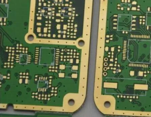
Immersion Gold vs Gold Plated PCB
The materials selected for Immersion Gold vs Gold Plated PCB play a pivotal role in determining the board’s electrical, thermal, and mechanical properties. While both surface finishes incorporate gold as a key element, the underlying layers and their interactions define the final performance.
Both Immersion Gold and Gold Plated PCBs are fabricated on copper-clad laminates. The copper layer provides excellent electrical conductivity and forms the foundation for subsequent plating. High-reliability designs often utilize rolled copper foil or electrolytic copper foil.
Rolled Copper Foil: Mechanically rolled to achieve a uniform thickness, this foil offers superior surface smoothness, better adhesion for plating, and enhanced mechanical strength. It is ideal for high-frequency applications where signal integrity is critical.
Electrolytic Copper Foil: Produced by an electrolytic deposition process, this type is more flexible and cost-effective. While slightly rougher in texture, it can improve adhesion for certain types of plating.
A defining feature of Immersion Gold is the electroless nickel layer beneath the gold. This nickel acts as a diffusion barrier, preventing copper from migrating into the gold layer, which could degrade solderability and increase the risk of corrosion. Typically, the nickel thickness ranges from 3 to 6 microns, providing both structural support and long-term stability.
The gold layer itself varies significantly between Immersion Gold and Gold Plated PCB finishes:
Immersion Gold: Gold is deposited chemically, forming a very thin layer—usually 0.05 to 0.1 microns—sufficient to prevent oxidation and maintain excellent solderability. Because the layer is thin, it minimizes the cost of gold while preserving performance.
Gold Plated PCB: Electroplating creates a thicker gold layer, often exceeding 1 micron, which is crucial for applications requiring frequent mechanical contacts, such as connectors or edge fingers. The thicker layer provides enhanced wear resistance but increases material cost.
Other materials, including surface coatings, fluxes, and solder masks, interact with the gold finish to influence wettability, adhesion, and resistance to environmental factors. High-reliability PCBs often require carefully selected solder masks and anti-oxidation treatments to complement the chosen surface finish.
By understanding the material composition of Immersion Gold vs Gold Plated PCB, designers can anticipate performance under operational stress, optimize manufacturing processes, and reduce potential failure modes in critical applications.
Understanding the manufacturing processes of Immersion Gold vs Gold Plated PCB is crucial for high-reliability design. The processes determine surface uniformity, solderability, mechanical durability, and overall board quality.
Immersion Gold, also known as ENIG (Electroless Nickel Immersion Gold), involves a multi-step chemical deposition process:
Copper Cleaning and Activation: The copper surface is first cleaned chemically to remove oxides and impurities. Proper cleaning ensures uniform nickel deposition and prevents adhesion issues.
Electroless Nickel Deposition: A chemical reaction deposits a uniform nickel layer over the copper traces. This nickel barrier prevents copper diffusion and provides a solid foundation for gold deposition.
Immersion Gold Deposition: The PCB is immersed in a gold solution, where a thin gold layer is chemically deposited onto the nickel surface. The process is self-limiting, resulting in precise and uniform gold thickness.
Rinsing and Drying: After gold deposition, boards are thoroughly rinsed and dried to remove residual chemicals, ensuring a clean and stable surface.
Advantages of the Immersion Gold Process:
Provides an ultra-flat surface, ideal for fine-pitch components.
Excellent solderability without additional fluxing.
Low gold consumption, reducing material cost while maintaining performance.
Gold Plated PCBs involve electroplating, where an electrical current deposits a thicker gold layer onto the board. Typical steps include:
Surface Preparation: The copper or nickel surface is cleaned and activated similarly to ENIG.
Strike Layer Application: A thin gold strike layer is applied to ensure adhesion and conductivity.
Electroplating of Gold: The PCB is placed in an electrolytic bath, and a thicker gold layer is plated over the strike layer. The plating time and current determine final thickness.
Rinsing and Post-Treatment: Boards are rinsed to remove residual electrolytes, and sometimes a protective coating is applied to enhance durability.
Advantages of the Gold Plated Process:
Offers a thicker gold layer suitable for high-cycle mechanical contacts.
Provides superior wear resistance for connectors and edge fingers.
Ensures long-term conductivity under repeated mating conditions.
In both processes, maintaining tight control over chemistry, temperature, and immersion times is essential. Minor deviations can cause:
Non-uniform gold thickness
Poor adhesion between layers
Increased susceptibility to corrosion or solderability issues
High-reliability applications often require third-party inspection, including X-ray fluorescence (XRF) measurement for gold thickness and surface profilometry to confirm flatness.
By carefully managing these processes, manufacturers can produce Immersion Gold and Gold Plated PCBs that meet stringent reliability standards. Trusted manufacturers like JM PCB have mastered these processes, combining precision control with scalable production to support both high-volume and specialized applications.
The surface finish of a PCB is critical to its solderability, signal integrity, and long-term reliability. Understanding the surface finish characteristics in Immersion Gold vs Gold Plated PCB helps engineers make informed decisions for high-reliability designs.
Immersion Gold: One of the most significant advantages of ENIG is its ultra-flat surface. The electroless nickel provides a smooth base, while the immersion gold adds a thin, uniform layer. This flatness is especially beneficial for fine-pitch and micro-BGA components, where uneven surfaces can lead to solder joint defects and electrical failures.
Gold Plated PCB: Electroplated gold typically results in a slightly thicker and less planar surface. While excellent for connector contacts and edge fingers, it may pose challenges in soldering ultra-fine components due to minor variations in thickness.
Surface roughness impacts solder wetting and adhesion:
Immersion Gold: The chemical deposition process yields a very smooth surface, minimizing micro voids and defects. This results in consistent solder wetting and reduced risk of open circuits.
Gold Plated PCB: Electroplated gold can produce a rougher texture depending on plating parameters, which may enhance adhesion in some cases but could affect fine-pitch soldering reliability.
Immersion Gold: Gold is highly resistant to oxidation, even in thin layers, preventing surface corrosion and maintaining solderability over time. The nickel layer beneath also acts as a protective barrier against copper diffusion.
Gold Plated PCB: Thicker gold layers provide excellent long-term resistance to oxidation and wear, particularly suitable for applications with frequent mechanical contacts or harsh environmental exposure.
Solderability is a key criterion for high-reliability PCBs:
Immersion Gold: Offers excellent solderability due to the flat, oxidation-resistant surface. Ideal for lead-free solder processes and high-density component placement.
Gold Plated PCB: While also highly solderable, the thicker gold layer may require careful flux selection and soldering profiles to avoid joint defects, especially in fine-pitch designs.
Immersion Gold: Suitable for applications with limited mechanical mating, such as surface-mounted devices (SMDs).
Gold Plated PCB: Preferred for connectors, edge fingers, and areas requiring repeated insertion cycles. The thicker gold layer ensures electrical continuity even after multiple contacts.
In summary, Immersion Gold vs Gold Plated PCB offers distinct surface finish characteristics tailored to different reliability and performance requirements. Choosing the right finish involves balancing flatness, solderability, and contact wear resistance according to the application’s specific needs.
Electrical performance is a crucial factor in high-reliability designs, particularly in applications such as aerospace, telecommunications, and medical electronics. Understanding the electrical performance of Immersion Gold vs Gold Plated PCB allows engineers to optimize signal integrity, minimize resistance, and ensure long-term reliability.
Immersion Gold: The gold layer is extremely thin, typically 0.05–0.1 microns, but sufficient to provide corrosion protection without significantly affecting the underlying copper’s conductivity. The nickel barrier ensures that copper does not diffuse into the gold, maintaining stable electrical resistance over time.
Gold Plated PCB: Electroplated gold layers are thicker, often exceeding 1 micron. This thickness provides excellent contact conductivity, particularly in areas with repeated mechanical connections. The thicker gold also reduces contact resistance variability, which is critical for high-speed connectors.
High-frequency signals are sensitive to surface roughness, layer uniformity, and metal composition:
Immersion Gold: The smooth surface of ENIG reduces signal scattering and insertion loss, making it suitable for high-frequency PCBs used in RF and microwave applications. Flatness and low roughness help maintain controlled impedance.
Gold Plated PCB: While electroplated gold offers excellent contact performance, the slightly rougher surface can introduce minor impedance variations in ultra-high-frequency circuits. Careful design and plating control mitigate these effects.
Immersion Gold: Best suited for boards with minimal mechanical mating, such as SMT components and fine-pitch ICs. Repeated contacts can wear through the thin gold layer, exposing the nickel or copper beneath.
Gold Plated PCB: The thicker gold layer supports frequent mating cycles in edge connectors, socketed components, or test points. Electrical performance remains consistent even after thousands of insertion/removal cycles.
Immersion Gold: Maintains stable conductivity across standard operating temperatures. ENIG’s thin gold layer does not contribute significantly to thermal expansion issues, making it compatible with lead-free soldering processes.
Gold Plated PCB: Thicker gold layers have slightly higher thermal mass but are generally reliable under typical PCB operating temperatures. Careful plating ensures the layer does not peel or crack during thermal cycling.
When evaluating Immersion Gold vs Gold Plated PCB, the choice depends on the application:
| Feature | Immersion Gold | Gold Plated PCB |
|---|---|---|
| Conductivity | Stable | Superior for frequent contacts |
| Signal Integrity | Excellent for fine-pitch & RF | Good, slight variation at very high frequency |
| Mechanical Mating | Limited | Excellent, durable |
| Thermal Stability | High | High |
High-reliability designs demand PCBs that can withstand both thermal stress and mechanical strain without degradation. Evaluating the thermal and mechanical reliability of Immersion Gold vs Gold Plated PCB is essential to ensure long-term performance in critical applications.
Immersion Gold: The thin gold layer contributes minimally to thermal expansion, allowing the board to maintain dimensional stability during soldering and operational temperature fluctuations. The underlying nickel barrier also provides structural support, reducing stress on copper traces.
Gold Plated PCB: Thicker electroplated gold layers slightly increase thermal mass, but proper plating adhesion and controlled nickel or copper underlayers prevent delamination. Gold Plated PCBs are capable of enduring repeated thermal cycling, making them suitable for connector interfaces in high-temperature environments.
Immersion Gold: Offers moderate mechanical durability, ideal for surface-mounted components and minimal handling during assembly. Excessive mechanical abrasion or repeated connector insertions can wear through the thin gold layer, exposing the nickel and potentially compromising reliability.
Gold Plated PCB: The thicker gold layer is highly resistant to mechanical wear, suitable for edge connectors, test points, and high-cycle mating applications. Electroplated gold maintains consistent contact performance even under repeated mechanical stresses.
Immersion Gold: Provides excellent oxidation resistance thanks to the inert nature of gold. The nickel barrier prevents copper diffusion, reducing the risk of surface corrosion over time. However, extreme environmental exposure, such as high humidity or salt spray, can challenge the thin layer.
Gold Plated PCB: Thicker gold electroplating enhances corrosion resistance further, making it ideal for harsh environmental conditions. Even after prolonged exposure, the electrical and mechanical performance remains largely unaffected.
Long-term reliability encompasses performance under thermal, mechanical, and environmental stress:
Immersion Gold: Best suited for fine-pitch components, RF applications, and devices with minimal mechanical wear. ENIG finishes offer predictable performance over years of standard operation.
Gold Plated PCB: Optimized for high-cycle connectors, edge fingers, and industrial applications. Electroplated gold provides superior durability, maintaining both electrical conductivity and mechanical integrity over extended operational life.
Designers must weigh Immersion Gold vs Gold Plated PCB based on expected thermal and mechanical loads:
Use Immersion Gold for fine-pitch SMT boards, RF/microwave circuits, and low-contact environments.
Use Gold Plated PCB for connectors, test points, and applications requiring frequent insertion/removal cycles or harsh environmental exposure.
When selecting a surface finish, cost considerations often influence design decisions, especially for high-reliability PCBs. Evaluating the cost of Immersion Gold vs Gold Plated PCB involves analyzing material expenses, manufacturing complexity, and long-term economic benefits.
Immersion Gold: The gold layer in ENIG is extremely thin (0.05–0.1 microns), which significantly reduces gold consumption and lowers material costs. The nickel barrier, while adding some expense, is relatively inexpensive compared to thick gold plating. Overall, ENIG offers an economical option for high-density and fine-pitch applications without compromising reliability.
Gold Plated PCB: Electroplated gold requires a much thicker layer, often exceeding 1 micron. This increased gold consumption substantially raises material costs, especially for large boards or designs with numerous edge connectors. The cost must be justified by the application’s need for mechanical durability and repeated contact performance.
Immersion Gold: The ENIG process involves precise chemical deposition, which requires controlled baths, accurate timing, and consistent process monitoring. While moderately complex, it is scalable and cost-effective for high-volume fine-pitch boards.
Gold Plated PCB: Electroplating is more labor- and time-intensive. Thickness control is critical, and additional inspections are often required to ensure uniform deposition. These factors increase production costs compared to ENIG.
Choosing the right surface finish can also influence lifecycle costs:
Immersion Gold: Lower initial material cost, excellent for boards with minimal mechanical wear, and suitable for automated assembly processes. Reduced gold usage translates into lower inventory and raw material expenses.
Gold Plated PCB: Higher upfront costs are offset by long-term durability. In applications requiring frequent mating cycles or exposure to harsh conditions, electroplated gold reduces maintenance and replacement costs, justifying the investment.
The decision should align cost with application requirements:
Opt for Immersion Gold in fine-pitch, low-contact, or high-density boards where solderability and flatness are paramount.
Opt for Gold Plated PCB in connector-heavy, high-cycle, or industrial boards where mechanical reliability outweighs the initial cost.
Choosing the appropriate surface finish is critical for applications where PCB reliability and performance are paramount. Understanding the applications of Immersion Gold vs Gold Plated PCB helps engineers design boards that meet stringent operational and environmental requirements.
Immersion Gold: Ideal for high-density avionics and communication boards where fine-pitch components, RF circuitry, and minimal mechanical contact are prevalent. ENIG ensures excellent solderability and flatness, critical for signal integrity in high-frequency systems.
Gold Plated PCB: Used in connectors, edge fingers, and test interfaces that experience repeated insertion cycles or exposure to vibration and thermal stress. The thicker gold layer ensures sustained contact reliability over time.
Immersion Gold: Suited for compact, high-density devices like pacemakers, imaging modules, and diagnostic electronics. Its smooth surface and corrosion resistance maintain reliable electrical performance in sensitive medical circuits.
Gold Plated PCB: Employed in connectors or interface boards that require repeated plugging/unplugging during device maintenance or testing, ensuring consistent electrical contact throughout the device lifespan.
Immersion Gold: Widely used in high-speed signal boards and RF modules where controlled impedance and fine-pitch assembly are essential. The thin, flat gold layer minimizes signal distortion and maintains signal integrity.
Gold Plated PCB: Applied to edge connectors, socketed transceivers, and high-cycle interface points. The thicker gold layer withstands continuous mechanical mating while maintaining low contact resistance.
Immersion Gold: Suitable for PCBs in control units, sensors, and low-contact signal boards. ENIG’s corrosion resistance ensures reliable performance in environments with moderate exposure to heat and humidity.
Gold Plated PCB: Preferred for connectors, relays, and test points in harsh environments where mechanical wear and frequent interfacing are common. Electroplated gold maintains conductivity and mechanical integrity under high vibration, temperature, and humidity.
Immersion Gold: Used in PCBs with high-density SMT components and low-mating contacts, such as measurement modules and signal conditioning boards.
Gold Plated PCB: Ideal for frequent-contact areas, such as probe pads, sockets, and edge connectors that undergo thousands of insertion/removal cycles during testing.
Understanding the step-by-step production process of Immersion Gold vs Gold Plated PCB is essential for engineers and designers seeking high-reliability PCBs. Each stage—from substrate preparation to final inspection—impacts performance, solderability, and durability.
Cleaning: Copper surfaces are thoroughly cleaned to remove oxides, oils, and contaminants. Proper cleaning is critical for adhesion and uniform deposition.
Etching and Patterning: Copper traces are formed through photolithography and chemical etching. The accuracy of these steps determines fine-pitch and high-density performance.
Surface Activation: Chemical activation ensures nickel or strike layers adhere effectively to the copper surface.
The PCB is immersed in a nickel plating solution.
A controlled chemical reaction deposits a uniform nickel layer, usually 3–6 microns thick.
Key process controls include bath temperature, pH, and immersion time to ensure consistent thickness and adhesion.
Immersion Gold (ENIG):
The board is immersed in a gold solution, where a thin gold layer (0.05–0.1 microns) is chemically deposited over nickel.
Self-limiting reactions ensure uniform coverage across traces and pads.
Gold Plated PCB:
A strike layer of gold is applied first to promote adhesion.
The board then undergoes electroplating, depositing a thicker gold layer (often >1 micron).
Plating parameters such as current density, time, and bath composition control layer thickness and uniformity.
After deposition, boards are thoroughly rinsed to remove residual chemicals.
Drying ensures no moisture remains, which could compromise solderability or lead to corrosion during storage.
X-ray Fluorescence (XRF): Measures nickel and gold layer thickness.
Surface Profilometry: Checks flatness and uniformity.
Electrical Testing: Confirms continuity and resistance parameters.
Mechanical Testing: Ensures adhesion and durability under thermal and mechanical stress.
Maintaining tight chemical and temperature controls minimizes defects such as non-uniform plating, peeling, or micro-voids.
Batch consistency is crucial for high-volume production, particularly in high-density and fine-pitch designs.
By following these step-by-step processes and adhering to stringent quality standards, designers can achieve PCBs that meet demanding high-reliability specifications while optimizing performance and longevity.
Understanding the advantages of Immersion Gold vs Gold Plated PCB helps engineers and designers select the appropriate surface finish for high-reliability applications. Each finish offers distinct benefits tailored to specific performance and operational requirements.
Flat and Smooth Surface:
Provides ultra-flat surfaces ideal for fine-pitch components, BGAs, and high-density boards.
Minimizes solder bridging and ensures consistent solder joint formation.
Excellent Solderability:
The inert gold surface resists oxidation, maintaining consistent wetting for lead-free and conventional soldering processes.
Reduces the need for additional flux or rework.
Cost Efficiency:
Thin gold layer consumes minimal gold, lowering material costs while maintaining high performance.
Economical for high-density and fine-pitch designs where mechanical wear is minimal.
Corrosion and Oxidation Resistance:
Gold’s inert properties prevent surface oxidation over time.
The underlying nickel barrier prevents copper diffusion and enhances long-term stability.
Durability Under Mechanical Stress:
Thick electroplated gold layer withstands repeated mating cycles in connectors, edge fingers, and socketed components.
Maintains electrical continuity after thousands of insertions/removals.
Enhanced Wear Resistance:
Suitable for harsh environments, including vibration, temperature extremes, and high-humidity conditions.
Ideal for industrial, automotive, and military applications requiring frequent handling.
Superior Contact Performance:
Low contact resistance ensures reliable signal transmission in connectors and test points.
Minimizes degradation over long-term operation, critical for high-reliability systems.
Long-Term Reliability:
Electroplated gold maintains mechanical and electrical integrity over extended periods, reducing maintenance and replacement costs.
When deciding between Immersion Gold vs Gold Plated PCB:
Use Immersion Gold for fine-pitch, RF, and high-density PCBs with minimal mechanical mating.
Use Gold Plated PCB for connectors, edge fingers, test points, and applications requiring repeated mechanical contact.
Selecting the appropriate surface finish is a critical decision in high-reliability PCB design. The choice between Immersion Gold vs Gold Plated PCB directly impacts solderability, mechanical durability, corrosion resistance, and overall electrical performance.
Immersion Gold (ENIG):
Provides an ultra-flat, smooth surface ideal for fine-pitch components and high-density boards.
Excellent solderability with lead-free and conventional solder processes.
Thin gold layer is cost-effective and corrosion-resistant but less suitable for repeated mechanical contact.
Gold Plated PCB:
Offers a thicker, more durable gold layer suitable for connectors, edge fingers, and high-cycle mating applications.
Superior wear resistance and long-term reliability under mechanical stress and harsh environmental conditions.
Slightly higher material and process costs, justified by enhanced durability and reduced lifecycle maintenance.
Designers should assess the application’s requirements:
For fine-pitch SMT boards, RF circuits, or low-contact applications, Immersion Gold is typically preferred.
For connector-heavy, high-cycle, or industrial environments, Gold Plated PCB ensures mechanical and electrical reliability.
Understanding common questions about Immersion Gold vs Gold Plated PCB helps designers make informed decisions regarding material selection, reliability, and process considerations.
Answer: Rolled copper foil is produced by mechanically rolling copper into thin sheets, offering better surface quality and mechanical strength. Electrolytic copper foil is deposited via an electrolytic process and is more flexible and cost-effective. Choice of copper foil impacts overall board reliability, surface roughness, and solderability.
Answer: Immersion Gold (ENIG) typically has a very thin gold layer (0.05–0.1 microns) over a nickel barrier, sufficient for solderability but less suited for frequent mechanical contacts. Gold Plated PCBs feature thicker electroplated gold (often >1 micron), providing enhanced mechanical durability and repeated mating resistance.
Answer: Immersion Gold is generally preferred for fine-pitch and high-density SMT components due to its ultra-flat surface and smoothness. Gold Plated PCB, while durable, may introduce minor surface roughness that could affect soldering in ultra-fine pitch assemblies.
Answer: Yes. Both finishes provide excellent corrosion resistance, but Gold Plated PCBs with thicker layers are more suitable for harsh environments with repeated mechanical wear, high humidity, or temperature extremes.
Answer: Gold thickness affects contact resistance, wear resistance, and long-term reliability. Thicker gold (electroplated) ensures consistent performance under repeated mating, while thinner immersion gold maintains excellent conductivity for soldering and low-contact applications without adding unnecessary material costs.


Connect to a Jerico Multilayer PCB engineer to support your project!
Request A Quote


 Quote
Quote