


+86 13603063656

Printed Circuit Board (PCB) manufacturing has always been a field where chemistry, physics, and engineering intersect to create the backbone of modern electronics. From the earliest single-layer boards in radios and calculators to today’s ultra-dense, multi-layered high-density interconnect (HDI) boards, the fabrication processes have evolved dramatically. Among these processes, etching is one of the most critical. It defines the copper patterns that ultimately serve as electrical pathways, dictating both the performance and the reliability of the finished product.
In the early decades of PCB manufacturing, acidic etching methods dominated. Ferric chloride and cupric chloride were widely used as etching solutions. They were effective but carried limitations: undercutting was difficult to control, fine-line resolution was often compromised, and the environmental impact was significant due to the waste generated. As the electronics industry demanded finer traces, higher yields, and lower environmental footprints, innovation in etching technologies became unavoidable.
This is where PCB Alkaline Etching entered the picture. Compared with its acidic counterparts, alkaline etching demonstrated superior control over line definition, minimized undercutting, and improved overall yield. With the rise of personal computers, mobile devices, automotive electronics, and aerospace systems, alkaline etching became the method of choice for manufacturers pushing the limits of circuit density.
My view is that this transition represents more than just a shift in chemistry—it symbolizes the broader transformation of the electronics industry. Manufacturers are no longer satisfied with “good enough” PCBs; instead, they demand consistency, reproducibility, and scalability. PCB Alkaline Etching directly addresses those needs.
PCB Alkaline Etching
The global electronics market is entering a new era, shaped by 5G, artificial intelligence, Internet of Things (IoT), autonomous vehicles, and advanced medical devices. These applications require printed circuit boards with extremely fine lines, high aspect-ratio vias, and robust performance under stress. In such a demanding context, etching precision is not optional—it is essential.
PCB Alkaline Etching matters today for several reasons:
Yield Optimization
In high-volume production, even a small improvement in yield translates to enormous cost savings. Alkaline etching reduces defect rates, particularly in fine-line applications, thereby supporting high-volume reliability.
Line Definition and Resolution
One of the most critical factors in advanced PCBs is the ability to produce fine lines with minimal undercutting. Acidic solutions often struggle here, whereas alkaline solutions provide a more controlled and uniform etch.
Compatibility with HDI and Next-Generation Boards
HDI boards, with microvias and ultra-fine traces, have become standard in smartphones and wearable devices. Alkaline etching is particularly well-suited to handle the tight tolerances these boards require.
Environmental Impact and Waste Management
Environmental regulations are becoming stricter worldwide. Alkaline etching solutions can be regenerated and recycled, making them more sustainable and cost-efficient in the long term compared to older chemistries.
Global Competitiveness
For PCB manufacturers competing in global markets, adopting advanced PCB Alkaline Etching is often the difference between being a second-tier supplier and being trusted by top-tier OEMs.
When I reflect on these drivers, I see a clear trend: PCB Alkaline Etching is no longer just an optional upgrade. It has become a necessity for companies seeking to remain competitive in a market that demands ever-smaller geometries, higher reliability, and environmental responsibility.
At the core of PCB Alkaline Etching lies a relatively simple chemical principle: copper, the conductive material in printed circuit boards, can be selectively dissolved in a strongly alkaline solution containing oxidizing agents. The most common etchant used is an aqueous solution of copper chloride (CuCl₂) in combination with ammonium chloride (NH₄Cl) or ammonium hydroxide (NH₄OH). The process relies on the ability of these solutions to oxidize metallic copper into soluble copper complexes.
In practice, the chemistry is slightly more complicated because regeneration is also part of the system. Fresh oxidants are introduced, or the solution is aerated to convert cuprous ions (Cu⁺) back to cupric ions (Cu²⁺), thus prolonging the bath’s lifetime. This regenerative capability is one of the reasons why alkaline etching is considered more sustainable compared to acidic alternatives.
What I find particularly elegant about PCB Alkaline Etching is that it achieves a delicate balance: strong enough to rapidly etch away exposed copper, but controlled enough to leave protected areas intact with minimal undercutting. This precision is not accidental; it is the result of decades of refinement in chemistry and equipment design.
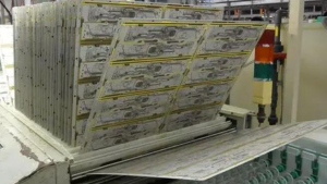
A typical PCB Alkaline Etching line consists of several integrated modules designed to handle the boards in a continuous and automated manner. While designs vary between equipment suppliers, the general flow includes:
Pre-cleaning
Boards are first cleaned with alkaline cleaners and mild mechanical scrubbing. This removes fingerprints, oxides, or resist residues that could interfere with uniform etching.
Resist Application and Patterning
A photoresist or dry film resist is applied to define the areas of copper that must remain. Advanced lithography ensures precise line definition.
Alkaline Etching Chamber
This is the heart of the system. Boards pass through spray chambers where high-pressure nozzles uniformly deliver the alkaline etchant across the copper surface. Parameters such as temperature, pressure, and flow rate are carefully controlled.
Regeneration and Filtration
As copper is dissolved, the etchant accumulates copper ions. To maintain performance, the solution is continuously regenerated—often by air oxidation or chemical additives—to restore the Cu²⁺ concentration. Filtration systems remove particulates to avoid nozzle clogging.
Stripping of Resist
After etching, the remaining photoresist is stripped off, revealing the final copper pattern.
Final Cleaning and Inspection
Boards undergo rinsing, drying, and visual or automated optical inspection (AOI) to verify pattern fidelity.
In my opinion, one of the most impressive aspects of PCB Alkaline Etching equipment is how it integrates real-time monitoring. Modern systems track parameters like copper concentration, pH, temperature, and spray pressure continuously. This automation minimizes operator error and ensures reproducibility across thousands of panels.
The choice between alkaline and acidic etching has long been debated in the PCB industry. Each has its place, but their strengths differ significantly.
1. Line Definition and Undercutting
Acidic etching tends to attack copper isotropically, meaning it dissolves copper equally in all directions. This results in more undercutting, which can compromise line width accuracy.
PCB Alkaline Etching, by contrast, is more anisotropic. It removes copper predominantly downward, preserving sharper edges and finer lines.
2. Yield and Reliability
In mass production, alkaline etching generally provides higher yields due to its controlled etch profile.
Acidic etching often requires additional process compensation (like over-dimensioning traces) to counteract undercutting, which adds complexity.
3. Environmental Considerations
Acidic etching generates large amounts of waste that require careful neutralization and disposal.
Alkaline solutions can be regenerated and recycled, significantly reducing both environmental impact and operating cost.
4. Cost Efficiency
Acidic systems may be cheaper initially, but over time, waste disposal and yield losses add up.
PCB Alkaline Etching provides better long-term cost efficiency, especially for HDI and fine-line production.
5. Application Suitability
Acidic etching is still used in inner-layer production for multilayer boards where line resolution is less critical.
PCB Alkaline Etching is the clear choice for outer layers, HDI, and advanced applications where precision is non-negotiable.
From my perspective, this comparison highlights a broader truth: technology adoption is rarely about what is “possible” but rather about what is “scalable and sustainable.” Acidic etching can still do the job, but PCB Alkaline Etching makes the process scalable for modern electronics manufacturing.
In PCB manufacturing, yield is arguably one of the most important performance metrics. Yield refers to the percentage of produced boards that meet quality standards without requiring rework or scrapping. Even a small improvement in yield—from, say, 92% to 96%—can save a manufacturer millions of dollars annually in a high-volume production environment.
PCB Alkaline Etching contributes directly to superior yield by minimizing defects such as:
Undercutting: Alkaline solutions etch copper more vertically than horizontally, reducing the loss of conductor width. This minimizes line breaks and shorts.
Over-etching: The controlled chemistry of alkaline baths avoids excessive copper removal, which is a common cause of open circuits.
Etch Non-Uniformity: Spray nozzles and carefully controlled fluid dynamics deliver a uniform etch across the entire panel, reducing variability between edges and center areas.
From a yield perspective, one of the biggest advantages is the repeatability of the process. When a manufacturer scales from prototyping to thousands of boards per day, consistency is critical. Acidic etching often shows more variability because of less efficient regeneration and higher sensitivity to contamination.
I think it is fair to say that yield improvement is not just about cost reduction but also about reliability. Customers in aerospace, automotive, and medical sectors require zero-defect PCBs. PCB Alkaline Etching helps manufacturers meet these stringent expectations, ensuring that boards pass AOI and electrical testing on the first attempt.
The phrase “fine lines” has become synonymous with modern PCB design. Smartphones, wearables, and advanced processors demand line widths as narrow as 30 microns (and shrinking). Achieving such resolution requires etching methods that can faithfully reproduce the intended copper geometry.
PCB Alkaline Etching is uniquely suited for this task:
Minimal Undercutting
Because alkaline etching tends to dissolve copper anisotropically, traces maintain nearly vertical sidewalls. This enables designers to specify narrower line widths without worrying that the etching process will distort them.
Superior Line Edge Definition
The surface tension and spray dynamics of alkaline systems result in smooth edges with fewer micro-notches. This is critical for high-frequency circuits where impedance consistency is required.
Support for High-Density Interconnect (HDI)
Fine-line capability is a cornerstone of HDI technology. By enabling narrower traces and spaces, alkaline etching allows more routing density per unit area, reducing the need for additional layers and keeping boards thinner and lighter.
Reduced Design Compensation
In acidic etching, designers often have to oversize traces to account for expected losses during processing. With alkaline etching, compensation is minimal, saving time in design iterations and improving first-pass accuracy.
From my perspective, fine-line fabrication is not only about pushing technical limits but also about opening new possibilities in product design. A smartphone that integrates more functions into a smaller form factor, or a medical implant that combines advanced sensing with wireless communication, owes much of its feasibility to PCB Alkaline Etching enabling fine geometries.
Sustainability has become a central theme in electronics manufacturing. Governments, customers, and even end-users are demanding greener production methods. PCB Alkaline Etching contributes positively to environmental goals in several ways:
Regeneration of Etchants
The chemistry allows continuous regeneration. Copper ions (Cu⁺) produced during etching can be oxidized back to Cu²⁺, extending bath life and reducing waste generation.
Reduced Hazardous Waste
Unlike ferric chloride systems, alkaline etching does not produce large volumes of sludge. The waste streams are easier to treat, lowering the burden on wastewater treatment plants.
Resource Recovery
The copper dissolved in the etchant can be recovered through electro-winning or precipitation methods. This recovered copper is often reused, contributing to a circular economy.
Compliance with Global Standards
For PCB manufacturers exporting to Europe, North America, and Japan, compliance with environmental regulations (e.g., RoHS, REACH) is critical. Alkaline etching aligns better with these frameworks than traditional acid-based systems.
In my opinion, sustainability is not just about compliance. It also serves as a competitive advantage. Customers increasingly favor suppliers who demonstrate environmental responsibility. By adopting PCB Alkaline Etching, manufacturers can position themselves as both technologically advanced and environmentally conscious—a combination that builds trust with global brands.
At first glance, some might assume that alkaline etching is more expensive because of the advanced equipment and chemical management systems required. However, a closer analysis reveals the opposite:
Higher Yield Reduces Scrap Costs
As mentioned earlier, improved yields mean fewer boards are scrapped or reworked. The cost savings here are substantial.
Lower Chemical Consumption
Regeneration means fewer fresh chemicals are required over the long term, lowering operating costs.
Reduced Downtime
Modern alkaline etching lines incorporate self-cleaning nozzles and continuous monitoring, reducing maintenance-related downtime. This supports higher throughput.
Less Design Overcompensation
Because alkaline etching is more precise, designers do not need to oversize traces, saving both time and material.
Competitive Pricing in Mass Production
When cost is analyzed on a per-panel basis, especially in HDI or fine-line production, PCB Alkaline Etching consistently demonstrates cost efficiency over acidic alternatives.
From a personal perspective, I see cost efficiency as a natural byproduct of technical excellence. When a process reduces waste, increases yield, and simplifies design, cost savings inevitably follow. It is not that alkaline etching was developed primarily to cut costs, but its precision and sustainability lead to a virtuous cycle where efficiency becomes a built-in advantage.
The consumer electronics sector is perhaps the most visible and demanding field for PCB innovation. Smartphones, tablets, laptops, and wearable devices are designed to be smaller, lighter, and more powerful each year. This relentless miniaturization directly translates into a need for finer traces, denser routing, and higher yields in PCB manufacturing.
PCB Alkaline Etching plays a central role in meeting these requirements:
Miniaturization of Devices
Fine-line capability enabled by alkaline etching allows circuit patterns as narrow as 30 microns, which is essential for fitting multiple functions—cameras, sensors, wireless modules—onto compact boards.
Consistency Across Mass Production
Consumer devices are produced in volumes of millions. Alkaline etching ensures consistent performance across batches, reducing the risk of returns or warranty claims.
Support for Advanced Packaging
Techniques like system-in-package (SiP) and chip-on-board (COB) require PCBs with extreme precision. Alkaline etching helps maintain the accuracy necessary for these integrations.
In my view, the success of global smartphone leaders is partially built on their suppliers’ mastery of PCB Alkaline Etching. Without this process, achieving the sleek, multifunctional devices we take for granted today would be nearly impossible.
Automobiles have evolved from mechanical machines into rolling computers. Modern vehicles contain dozens of electronic control units (ECUs) that manage everything from engine performance to safety systems like anti-lock brakes and airbags. With the rise of electric vehicles (EVs) and autonomous driving, the demand for robust and reliable PCBs has increased exponentially.
Here, PCB Alkaline Etching contributes in several ways:
Reliability Under Harsh Conditions
Automotive electronics must withstand high temperatures, vibrations, and exposure to chemicals. By reducing etch defects, alkaline etching ensures robust trace integrity, lowering the risk of field failures.
Support for High-Current Applications
Power electronics in EVs require thick copper PCBs with precisely etched wide traces. Alkaline etching handles these requirements with better uniformity than acidic methods.
Safety-Critical Performance
Any failure in automotive electronics can have life-or-death consequences. High-yield processes like alkaline etching are essential to meet stringent safety standards (ISO 26262).
From my perspective, automotive electronics illustrate why yield and reliability matter just as much as cost. A defective board in a consumer gadget may be inconvenient, but in a vehicle, it could be catastrophic. PCB Alkaline Etching provides the consistency required for this sector.
HDI PCBs are a cornerstone of next-generation electronics. They enable higher wiring density by using finer lines, smaller vias, and stacked microvias. These features are critical in devices where space is limited but performance demands are high—such as smartphones, 5G base stations, and advanced medical equipment.
PCB Alkaline Etching is almost indispensable in HDI production because:
Fine-Line Capability
HDI designs often require line widths and spaces below 50 microns. Alkaline etching delivers these geometries with minimal distortion.
Reduced Layer Count
By enabling finer routing, alkaline etching allows designers to fit more circuits per layer. This can reduce the overall number of PCB layers, lowering cost and thickness.
Signal Integrity
High-frequency applications demand consistent impedance. Smooth, well-defined traces produced by alkaline etching contribute directly to better electrical performance.
In my opinion, HDI represents the point where traditional PCB processes simply cannot keep up. Without PCB Alkaline Etching, the complexity of today’s smartphones and communication devices would not be feasible.
The aerospace and defense industries are among the most demanding when it comes to PCB performance. Systems such as radar, avionics, and satellite communications require absolute reliability under extreme conditions.
PCB Alkaline Etching supports these industries in several key ways:
Precision and Reliability
Military-grade PCBs often involve ultra-fine traces for high-frequency circuits. Alkaline etching provides the required precision while maintaining robustness.
Resistance to Harsh Environments
PCBs in aerospace must survive extreme temperature cycles, radiation exposure, and mechanical stress. Reducing defects during etching is critical for such resilience.
Compliance with Military Standards
Boards must meet MIL-SPEC or equivalent requirements. The high yield and process control of alkaline etching make compliance more achievable.
What stands out to me is that aerospace and defense systems often push technology several years ahead of consumer markets. By adopting PCB Alkaline Etching, these industries not only ensure mission-critical reliability but also pave the way for techniques that eventually trickle down to commercial applications.
After exploring the technical foundations, industrial applications, comparative analysis, challenges, case studies, and broader reflections, one truth is clear: PCB Alkaline Etching is the cornerstone of modern PCB manufacturing.
It enables superior yield by reducing scrap and ensuring consistent panel-to-panel performance.
It supports fine-line definition, allowing designs to meet the ever-shrinking geometries of smartphones, automotive electronics, aerospace systems, and beyond.
It embodies sustainability, offering recyclability of copper and cleaner chemical management compared to traditional acidic methods.
It demonstrates industrial scalability, handling both prototypes and high-volume production with equal efficiency.
From my perspective, PCB Alkaline Etching is more than just a process—it is a strategic enabler of the electronics industry. Without it, the ambitions of 5G, AI hardware, and future IoT ecosystems would remain theoretical.
Rolled copper foil: Produced by mechanically rolling copper into thin sheets, offering superior surface quality, ductility, and mechanical strength. It is ideal for flexible PCBs.
Electrolytic copper foil: Produced by electrodeposition, it is more economical and offers excellent uniformity, making it the standard choice for rigid PCBs.
PCB Alkaline Etching produces straighter sidewalls, smoother line edges, and less undercutting compared to acidic etching. This makes it ideal for high-density interconnects (HDI), RF circuits, and any design requiring fine-line resolution. Additionally, copper recovery is easier with alkaline systems, which improves sustainability.
Consumer electronics: Smartphones, wearables, tablets.
Automotive: Advanced driver assistance systems (ADAS), radar, EV power electronics.
Aerospace & defense: Radar systems, avionics, mission-critical electronics.
Telecommunications: 5G base stations, optical networking equipment.
IoT and AI hardware: Devices demanding miniaturization and high signal integrity.
Copper recovery: Dissolved copper can be reclaimed and reused.
Reduced waste: Compared to acidic etching, alkaline processes generate less hazardous sludge.
Worker safety: Closed-loop systems limit operator exposure.
Energy efficiency: Optimized etching reduces rework and improves yield, indirectly lowering energy consumption.
Yes. Many smaller firms rely on specialized manufacturers such as JM PCB. By outsourcing production, they gain access to advanced etching technologies without the capital investment or maintenance burden. This model levels the playing field, allowing startups and SMEs to compete in high-tech markets.


Connect to a Jerico Multilayer PCB engineer to support your project!
Request A Quote


 Quote
Quote