


+86 13603063656
For decades, traditional single-pass lamination served the PCB industry remarkably well. It aligned perfectly with simpler layer counts, larger feature sizes, and relatively forgiving electrical requirements. However, modern electronics no longer operate within those boundaries.
High-speed computing, advanced networking equipment, automotive electronics, and heterogeneous integration all demand tighter interconnect density, shorter signal paths, and stricter reliability margins. Under these constraints, single-pass lamination begins to show fundamental limitations—not because it is flawed, but because it was never designed for such architectural complexity.
This is where Sequential PCB Manufacturing emerges—not as an incremental improvement, but as a structural rethinking of how complex PCBs are built. In my view, sequential manufacturing represents a philosophical shift: from stacking layers all at once to engineering interconnections step by step.

Sequential PCB Manufacturing
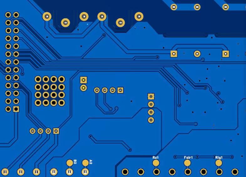
Sequential PCB Manufacturing refers to a fabrication methodology in which layers, interconnects, and vias are built through multiple lamination and processing cycles, rather than a single lamination step.
Instead of pressing all copper layers and dielectric materials together at once, this approach allows manufacturers to:
Build an initial core
Add new dielectric layers
Drill and metallize vias
Repeat lamination selectively
This stepwise approach enables microvias, buried vias, and stacked via architectures that are simply not feasible with traditional single-pass lamination.
From an engineering standpoint, Sequential PCB Manufacturing transforms the PCB from a static stack-up into a progressively constructed system.
Sequential PCB Manufacturing did not appear overnight. Its roots can be traced to early HDI (High-Density Interconnect) development, when mechanical drilling reached its physical limits.
Key evolutionary milestones include:
Transition from through-holes to blind and buried vias
Adoption of laser drilling for microvias
Demand for higher layer counts in constrained footprints
Initially, sequential processes were expensive and niche. Today, they are mainstream enablers for advanced electronics, driven by volume demand rather than experimental design.
The fundamental difference lies in process philosophy.
| Aspect | Conventional Lamination | Sequential PCB Manufacturing |
|---|---|---|
| Lamination cycles | Single | Multiple |
| Via types | Mostly through-hole | Blind, buried, stacked |
| Design flexibility | Limited | High |
| Yield sensitivity | Lower initially | Higher but controllable |
| Scalability | Layer-count dependent | Architecture dependent |
One of the most powerful benefits of Sequential PCB Manufacturing is layer-specific optimization.
Each lamination cycle allows:
Independent dielectric thickness control
Selective via placement
Fine-tuned impedance management
This precision is especially valuable for high-speed signal layers, where even minor variations can lead to signal degradation or timing skew.
As data rates continue to climb into tens and even hundreds of gigabits per second, signal integrity has become a dominant design constraint rather than a secondary consideration. One of the most profound yet often underappreciated benefits of Sequential PCB Manufacturing lies in how it reshapes the electrical behavior of interconnects.
By enabling blind and buried vias to be constructed incrementally, Sequential PCB Manufacturing significantly reduces via stubs. Shorter stubs mean:
Lower signal reflection
Reduced impedance discontinuities
Cleaner eye diagrams at high frequencies
In conventional single-pass lamination, designers are often forced to accept unnecessary via length simply because all layers are pressed at once. Sequential builds, in contrast, allow vias to terminate exactly where they are needed—no more, no less.
Power integrity challenges grow in parallel with signal density. As core voltages drop and current demand rises, even small inductive effects in vias and planes can lead to unacceptable voltage ripple.
Sequential PCB Manufacturing improves power integrity in several subtle but impactful ways:
Thinner dielectric layers between power and ground planes
Reduced loop inductance through stacked microvias
More flexible placement of decoupling capacitors close to active devices
The ability to sequentially add power layers allows designers to localize energy storage and distribution, rather than relying on globally shared planes that may introduce noise coupling.
In advanced designs I have reviewed, sequential builds often make the difference between a marginal power delivery network and a robust one.
Material choice becomes more complex—but also more powerful—under Sequential PCB Manufacturing.
Each lamination cycle introduces an opportunity to:
Use different resin systems
Adjust glass styles
Optimize dielectric constant (Dk) and dissipation factor (Df) per layer group
For example, low-loss materials can be reserved exclusively for high-speed signal layers, while standard FR-4 variants may still be used in mechanically supportive regions of the stack-up. This hybrid approach helps balance performance and cost.
In my opinion, material flexibility is one of the most underrated advantages of Sequential PCB Manufacturing, especially for cost-sensitive high-performance designs.
The evolution from single-pass lamination to Sequential PCB Manufacturing marks more than a change in fabrication technique—it reflects a fundamental shift in how engineers think about PCB architecture.
Traditional PCB manufacturing treated the board as a static stack of layers, optimized primarily for manufacturability and cost efficiency. That model worked well when signal speeds were moderate, interconnect density was manageable, and electrical margins were forgiving. Today, those assumptions no longer hold. Performance, reliability, and form factor constraints have converged to a point where manufacturing strategy directly shapes electrical and mechanical outcomes.
Sequential PCB Manufacturing answers this challenge by introducing intentionality into the vertical dimension of PCB design. Instead of accepting compromises imposed by one-time lamination, designers and manufacturers gain the ability to engineer interconnects, materials, and layer relationships progressively. This stepwise approach unlocks finer control over signal integrity, power delivery, and long-term reliability—capabilities that are increasingly non-negotiable in advanced electronics.
From my perspective, the most important value of Sequential PCB Manufacturing is not any single technical advantage, but the freedom it grants system architects. Freedom to localize performance-critical structures. Freedom to balance cost and capability through selective material usage. Freedom to align PCB fabrication more closely with semiconductor packaging trends rather than legacy board constraints.
At the same time, this freedom comes with responsibility. Sequential PCB Manufacturing amplifies both good and bad decisions. Success depends on disciplined design practices, realistic DFM strategies, and close collaboration with experienced fabricators. In this context, the role of the PCB manufacturer evolves from a passive supplier to an active engineering partner, capable of translating architectural intent into reliable physical reality.
Looking ahead, as chiplet architectures, heterogeneous integration, and higher-speed interfaces continue to blur the boundary between packaging and PCB fabrication, Sequential PCB Manufacturing will only grow in strategic importance. It is not merely a solution for today’s complexity—it is a foundation for the next generation of electronic systems.
In short, moving beyond single-pass lamination is not about doing more steps. It is about building smarter, layer by layer, with purpose, precision, and a long-term view of performance and reliability.
1. How should designers prepare for Sequential PCB-Manufacturing?
Early supplier engagement, disciplined stack-up planning, and realistic DFM constraints are essential.
2. Is Sequential PCB-Manufacturing only used for HDI boards?
No. While HDI designs benefit greatly, sequential processes are increasingly used in high-layer-count and high-reliability boards as well.
3. Does Sequential PCB-Manufacturing always increase cost?
Not necessarily. When evaluated at the system level, it often reduces overall cost by improving performance and reliability.
4. How many lamination cycles are typical in Sequential PCB-Manufacturing?
This depends on design complexity, but two to four cycles are common in advanced applications.
5. What are the main reliability risks in Sequential PCB-Manufacturing?
Poor via design, inadequate resin control, and insufficient process discipline are the primary risks.


Connect to a Jerico Multilayer PCB engineer to support your project!
Request A Quote


 Quote
Quote