


+86 13603063656
Stencils are a key enabling technology in PCB assembly, particularly in the application of solder paste during surface mount technology (SMT) processes. Their primary function is to control the amount and placement of solder paste applied to the PCB pads before component placement.
The precision of the stencil directly affects solder joint quality, production yield, and overall product reliability. Whether manufacturing a small batch prototype or launching a mass production run with tens of thousands of units, the stencil’s design and quality remain fundamental to success.
Stencils
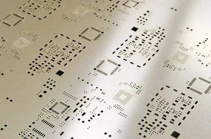
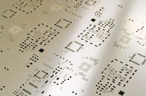
A stencil, in the context of PCB manufacturing, is a thin sheet—usually made of stainless steel—with laser-cut apertures matching the pattern of the PCB’s solder pads. During assembly, the stencil is placed over the PCB substrate, and solder paste is applied and spread across the stencil surface. The solder paste passes through the apertures, depositing precise amounts on the corresponding pads.
Stencils can vary by material, thickness, aperture design, and manufacturing technique. Common materials include:
Stainless steel: The most common material due to its durability, precision, and resistance to corrosion.
Nickel: Used for specialized applications requiring enhanced durability.
Polyimide films: Sometimes used for prototypes or specific low-volume applications.
The thickness of the stencil determines the volume of solder paste deposited. Typical thicknesses range from 100 microns to 200 microns, with variations depending on the component size and type.
The aperture geometry is a critical factor affecting solder paste volume and distribution. Aperture shapes can be simple squares or circles, or more complex shapes like trapezoids and chamfers to improve paste release and reduce defects.
Advanced design techniques such as electro-polishing of apertures and nano-coating can enhance stencil performance, leading to smoother paste release and longer stencil life.
In modern SMT assembly lines, stencils are integral to the solder paste printing stage. Automated stencil printers apply paste through the stencil, followed by pick-and-place machines that position components precisely on the freshly deposited paste. A high-quality stencil ensures uniform paste deposition, which directly influences solder joint integrity.
Using stencils in PCB assembly offers multiple significant benefits:
Stencils enable consistent solder paste volume and placement, reducing variability from one PCB to another. This precision is critical for maintaining high yields and minimizing rework or defects.
Stencil printing is a highly efficient process, allowing rapid solder paste application on complex boards with high component density. This speeds up the entire assembly process, essential for mass production environments.
Accurate paste volume and placement promote reliable solder joints, reducing common issues such as solder bridges, tombstoning, or insufficient solder.
By minimizing defects and rework, stencil use can significantly reduce production costs over time, despite initial investment in stencil manufacturing.
Stencils can be quickly designed and manufactured for new PCB layouts, enabling fast prototyping and smooth transition to production.
The process begins with detailed design work, where the PCB CAD files are analyzed, and the stencil apertures are defined. This step requires expertise to optimize aperture size and shape based on pad geometry and component types.
Most stencils today are made by laser cutting, which offers high precision and flexibility. Some advanced stencils incorporate electro-polished apertures or special coatings to improve performance.
After manufacturing, stencils undergo inspection to verify aperture accuracy and surface finish. Any deviation can affect solder paste volume and printing quality.
During PCB assembly, the stencil is aligned with the PCB and secured in the printing machine. Solder paste is applied with a squeegee across the stencil surface, forcing paste through apertures onto the PCB pads.
S-tencils require regular cleaning to remove solder paste residues, which could clog apertures and degrade print quality. Proper maintenance extends stencil life and ensures consistent results.
Transitioning from prototype builds to mass production introduces new demands on stencil design and usage:
Prototyping Phase: Stencils may be thinner or simpler to accommodate low-volume runs and fast design iterations.
Pilot Production: Stencils are optimized for production speed and reliability, sometimes incorporating additional features like nano-coatings.
Mass Production: High durability, precise apertures, and rigorous quality control become paramount. Stencils must maintain consistent printing over large volumes without degradation.
At JM PCB, their expertise in providing tailored stencil solutions supports clients through each production stage. Their ability to deliver both prototype and production stencils helps manufacturers maintain quality and efficiency across the board.
While stencils are essential, they come with challenges:
Aperture clogging: Paste residue can clog apertures, leading to defects.
Misalignment: Improper alignment between stencil and PCB causes paste misplacement.
Wear and tear: Over time, stencil apertures may degrade, affecting print quality.
Material limitations: Different PCB designs and paste formulations may require specialized stencil materials or coatings.
Choosing a reputable supplier like JM PCB, with advanced manufacturing capabilities and quality assurance, can help mitigate these challenges.
S-tencils represent a vital bridge between PCB design and successful assembly, especially as production scales from prototypes to mass manufacturing. Their role in controlling solder paste deposition is fundamental to product reliability and yield.
From my experience, investing time in selecting and maintaining high-quality stencils pays off through fewer defects, reduced rework, and faster production cycles. It is no surprise that leading manufacturers rely on expert stencil providers like JM PCB to navigate this complex aspect of PCB assembly.
As electronics continue to evolve with higher density and finer pitch components, stencil technology must advance in parallel. Keeping up with these developments is essential for any manufacturer aiming to maintain competitive advantage.
Q1: What is the difference between rolled copper foil and electrolytic copper foil?
Rolled copper foil is produced by mechanically rolling copper into thin sheets, offering better surface quality and mechanical strength. Electrolytic copper foil is deposited via an electrolytic process and is more flexible and cost-effective.
Q2: How often should stencils be cleaned during production?
Stencils should be cleaned regularly, ideally after every 50 to 100 prints, depending on the solder paste used and the production environment. Regular cleaning prevents aperture clogging and maintains print quality.
Q3: Can the same stencil be used for different PCB designs?
Generally, stencils are custom-made for each PCB layout due to the unique pad configurations. Using the correct stencil ensures precise paste deposition and reduces defects.
Q4: What factors influence the choice of stencil thickness?
Stencil thickness depends on the size of PCB pads and the volume of solder paste required. Smaller pads need thinner stencils for precise paste control, while larger pads may require thicker stencils to deposit enough solder.
Q5: Are there alternatives to stainless steel for stencil materials?
While stainless steel is the most common, nickel and polyimide film stencils are alternatives for specific use cases, such as enhanced durability or low-volume prototyping.


Connect to a Jerico Multilayer PCB engineer to support your project!
Request A Quote


 Quote
Quote