


+86 13603063656
Transistor Circuit Boards stand at the very heart of modern electronics, shaping the way devices function, communicate, and evolve. Without them, the smartphones we rely on, the industrial machines that power global manufacturing, and the satellites that connect continents would simply not exist. At their core, these circuit boards provide the physical and electrical framework in which transistors—the essential semiconductor switches—operate efficiently.
The shift from vacuum tubes to transistors in the mid-20th century transformed electronics into a more compact, efficient, and scalable industry. But what makes this transformation sustainable today is not only the transistor itself but the Transistor Circuit Boards that integrate millions (and now billions) of transistors into cohesive systems. These boards transform abstract semiconductor design into tangible, functioning hardware.
In my own analysis, what makes Transistor Circuit Boards so critical is not only their role as passive carriers of circuits but as active enablers of system-level integration. They dictate the electrical performance, signal integrity, thermal reliability, and even product longevity. Every decision—from copper thickness to substrate material—directly impacts the final product’s success.
Transistor Circuit Boards
The story of Transistor Circuit Boards is closely intertwined with the overall history of electronics. Before transistors, vacuum tubes dominated circuits. They were bulky, power-hungry, fragile, and limited in scaling. When transistors emerged in the late 1940s, engineers suddenly had a component that was smaller, more efficient, and could be mass-produced. However, the transistor alone was not enough. It needed a platform—a structured medium—that could host, connect, and protect it in larger systems. That platform evolved into what we now recognize as Transistor Circuit Boards.
In the 1950s, the earliest printed circuit boards (PCBs) were simple, single-sided layouts, mostly designed for radio and military communication equipment. Transistors were mounted through holes, with wires soldered manually. Reliability was inconsistent, but compared to the tangled wiring of earlier systems, it was revolutionary.
By the 1960s, double-sided boards appeared, and plated-through holes allowed for more compact layouts. This directly benefited Transistor Circuit Boards, as designers could place transistors closer together, reducing parasitic effects and improving performance. Consumer electronics such as televisions and early calculators adopted this technology, driving mass demand.
The 1970s and 1980s marked the rise of multilayer boards. With integrated circuits becoming more complex, transistor density skyrocketed. Transistor Circuit Boards transitioned from being simple carriers to sophisticated platforms supporting signal integrity, power distribution, and thermal control. During this period, industries like aerospace and computing began to demand reliability far beyond consumer standards. As a result, innovations such as solder mask, surface-mount technology, and improved laminates appeared.
By the 1990s and 2000s, globalization accelerated PCB manufacturing, and Transistor Circuit Boards became ubiquitous in nearly every electronic device. The boards not only housed discrete transistors but also supported microprocessors with millions of transistors. The evolution wasn’t merely technical but economic. PCB fabrication hubs emerged in Asia, reducing cost while improving production scalability. Companies like JM PCB took advantage of these trends by offering tailored production capabilities for both high-end industries and consumer-grade markets.
Today, in the 2020s, the evolution continues with high-density interconnects (HDI), flexible and rigid-flex designs, and materials optimized for 5G and high-frequency applications. These changes are all designed to meet the relentless growth of transistor counts while keeping devices smaller, faster, and more energy-efficient. In essence, the history of Transistor Circuit Boards mirrors the progress of human technology itself—from bulky analog devices to compact, connected digital ecosystems.
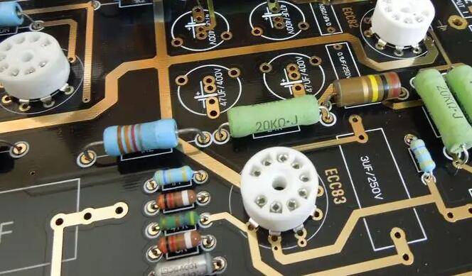
Understanding the anatomy of Transistor Circuit Boards is essential for grasping how they function. While PCBs may look like simple green plates to the untrained eye, they are intricate, multilayered structures carefully designed to balance electrical performance, mechanical strength, and manufacturability.
At the foundation of Transistor Circuit Boards lies the substrate. The most common material is FR4, a fiberglass-reinforced epoxy laminate. It provides electrical insulation and mechanical stability. However, as transistor density and operating frequencies increase, FR4 is not always sufficient. High-performance substrates such as Rogers laminates or polyimide are often used. These materials offer lower dielectric loss, better thermal stability, and improved reliability.
Copper is the lifeblood of Transistor Circuit Boards. Conductive layers etched into precise pathways form the circuitry that connects transistors, capacitors, resistors, and integrated circuits. The thickness of the copper (often measured in ounces per square foot) is carefully chosen depending on the current-carrying requirements. For high-power circuits, thicker copper ensures reduced resistance and better heat dissipation.
Above the copper layers, a solder mask is applied. This thin polymer coating insulates traces, prevents accidental solder bridging, and protects the copper from oxidation. The green color most people associate with circuit boards comes from this solder mask. On top of it, silkscreen printing adds component labels, test marks, and logos, helping engineers identify and assemble components correctly.
One of the defining features of Transistor Circuit Boards is how transistors are mounted. In the early years, through-hole mounting was dominant. Wires from transistors passed through drilled holes and were soldered on the opposite side. Today, surface-mount technology (SMT) dominates, enabling smaller footprints, higher density, and automated assembly. Transistors in SMT form are placed directly onto pads using solder paste, then reflowed in ovens.
To ensure stable operation of transistors, Transistor Circuit Boards typically include dedicated power and ground planes. These continuous copper sheets reduce voltage drops, minimize electromagnetic interference, and allow high-speed transistors to switch reliably without noise-induced errors.
Heat is one of the biggest enemies of transistor performance. As transistors switch, they generate heat that must be dissipated. Thermal vias, heat sinks, and even integrated copper planes are commonly employed. In more advanced boards, thermal interface materials and metal-core substrates help manage excessive heat, ensuring long-term stability.
With high-frequency applications such as 5G, radar, and computing, Transistor Circuit Boards must be designed to preserve signal quality. Trace width, spacing, dielectric constant, and impedance matching become critical. A poorly designed board can lead to crosstalk, reflections, and data corruption.
The structure of Transistor Circuit Boards is not only about physical layers but also about manufacturability. Typically, a workflow includes:
CAD design of transistor placement and routing.
Photolithographic patterning of copper traces.
Etching unwanted copper.
Laminating multiple layers together.
Drilling and plating vias.
Applying solder mask and silkscreen.
Assembling transistors and components via reflow or wave soldering.
Testing for electrical continuity and reliability.
Here, working with an experienced partner like JM PCB can significantly streamline the process. Their expertise in multilayer builds and advanced materials ensures that the structural integrity of Transistor Circuit Boards meets the increasingly demanding requirements of modern electronics.
The choice of materials in Transistor Circuit Boards is one of the most critical factors that determine their electrical, mechanical, and thermal performance. Since transistors are highly sensitive semiconductor devices, the surrounding board must provide a stable environment that minimizes electrical noise, dissipates heat effectively, and ensures long-term durability.
The substrate forms the physical backbone of Transistor Circuit Boards. The most commonly used substrate is FR4, a woven fiberglass cloth impregnated with epoxy resin. It offers a balanced trade-off between cost, performance, and manufacturability.
However, in applications where transistors operate at higher frequencies or in harsher environments, other materials are required:
Polyimide laminates – Known for high thermal resistance, they are often used in aerospace or automotive environments where reliability under extreme heat is critical.
Rogers laminates – Designed for high-frequency applications (RF and microwave), these substrates offer low dielectric loss, making them ideal for transistor circuits in 5G and radar systems.
Metal-core laminates (MCPCBs) – Used where heat dissipation is paramount, such as in power transistor circuits or LED drivers.
The dielectric constant (Dk) and dissipation factor (Df) of these substrates must be carefully matched with transistor switching frequencies to minimize signal loss.
The conductive layer in Transistor Circuit Boards is almost universally copper due to its excellent balance of conductivity, ductility, and cost-effectiveness. However, different forms of copper foil influence performance:
Rolled copper foil – Mechanically rolled, offering smoother surfaces and higher mechanical strength, often used in flexible transistor boards.
Electrolytic copper foil – Produced through an electrochemical deposition process, it offers excellent flexibility and is more cost-effective for mass production.
Engineers must balance copper thickness against manufacturing constraints. Too thin, and the board risks overheating; too thick, and etching fine traces for transistor connections becomes difficult.
Surface finishes protect exposed copper pads and ensure reliable solderability when mounting transistors. Common finishes include:
HASL (Hot Air Solder Leveling) – Traditional and cost-effective, though less suitable for fine-pitch transistor circuits.
ENIG (Electroless Nickel Immersion Gold) – Provides excellent planarity and oxidation resistance, making it popular for precision transistor circuits.
OSP (Organic Solderability Preservative) – A low-cost, environmentally friendly option suitable for simpler transistor boards.
The solder mask prevents solder bridging and oxidation, while conformal coatings (such as acrylic or silicone) protect Transistor Circuit Boards in harsh environments. For transistors used in automotive or outdoor applications, coatings are essential to prevent moisture-induced failures.
Since transistors generate significant heat, thermal management is crucial. Designers often integrate:
Thermal vias to conduct heat to inner or bottom layers.
Heat spreaders to dissipate localized heat.
TIMs (Thermal Interface Materials) such as pads or gels for direct coupling to heat sinks.
In summary, material selection in Transistor Circuit Boards is not a one-size-fits-all decision. It requires balancing cost, electrical properties, and environmental demands. This is why many engineers turn to experienced manufacturers like JM PCB, who provide guidance on the best laminates, copper foils, and finishes for specific transistor applications.
The manufacturing process of Transistor Circuit Boards is a multi-step sequence requiring precision, cleanliness, and quality control. Even the smallest defect—such as misaligned vias or uneven copper thickness—can affect transistor performance dramatically.
The process begins with electronic design automation (EDA) software, where engineers design transistor placement, trace routing, and layer stack-ups. Key considerations include:
Ensuring power and ground planes are sufficient for transistor switching.
Matching impedance for high-frequency transistor circuits.
Designing thermal relief for heat-sensitive transistors.
Sheets of laminate (FR4, polyimide, or other chosen materials) are cut to size. Copper foil is then laminated onto the substrate under high temperature and pressure, forming the base conductive layer.
A photoresist is applied over the copper surface. Using ultraviolet light, circuit patterns are transferred from design files to the resist. Unexposed areas are developed away, and the exposed copper is chemically etched, leaving precise traces to interconnect transistors and other components.
Holes are drilled where vias (vertical interconnections) or through-hole transistor leads will be placed. Laser drilling is used for microvias in HDI Transistor Circuit Boards. The inner walls of vias are plated with copper to establish reliable electrical connections between layers.
For complex transistor circuits, multiple etched layers are stacked together. Heat and pressure bond the layers into a single, rigid board. Misalignment at this stage can render the board useless, highlighting the need for precision.
A solder mask is applied to protect traces and define soldering pads for transistors. Silkscreen printing then adds labels, component outlines, and test markings.
Depending on the application, the board receives HASL, ENIG, or OSP surface finishes to prepare it for component assembly.
Transistors and other components are mounted either by:
Through-hole soldering for large or high-power transistors.
Surface-mount technology (SMT) for compact, high-density transistor circuits.
Automated pick-and-place machines ensure accurate placement, followed by reflow soldering.
Every Transistor Circuit Board undergoes electrical testing to check continuity, insulation resistance, and impedance. More advanced tests include:
In-circuit testing (ICT) – Checks individual transistor connections.
Automated optical inspection (AOI) – Detects soldering defects.
Functional testing – Simulates real operating conditions.
Some industries require additional steps such as conformal coating, underfill for SMT transistors, or potting for harsh environments.
The electrical performance of Transistor Circuit Boards is a defining factor in whether a device succeeds or fails in the real world. Since transistors function as switches or amplifiers, their operation depends heavily on the quality of signal transmission, power distribution, and noise suppression across the board.
One of the foremost concerns in designing Transistor Circuit Boards is maintaining signal integrity. Transistors switch at nanosecond speeds, meaning even minor disruptions can cause significant issues such as jitter, crosstalk, and reflections. To ensure stability:
Controlled impedance routing is applied, especially in high-frequency circuits.
Differential pair routing reduces noise for transistor-driven communication lines.
Proper grounding ensures return currents flow predictably, minimizing electromagnetic interference (EMI).
Transistors are highly sensitive to voltage fluctuations. A noisy power rail can compromise switching thresholds and introduce errors. Designers therefore use:
Dedicated power planes to provide low-resistance current paths.
Decoupling capacitors strategically placed near transistors to absorb transient spikes.
Low-inductance vias to reduce delays in current delivery.
Different transistor applications impose different frequency demands on circuit boards:
Low-frequency transistor circuits (e.g., power amplifiers) prioritize current capacity and heat dissipation.
High-frequency transistor circuits (e.g., RF amplifiers, 5G modules) demand substrates with low dielectric loss to avoid attenuation.
Digital transistor circuits require precise impedance control to ensure clock signals remain synchronized.
As transistor density increases, traces on Transistor Circuit Boards run closer together. This proximity increases the risk of unwanted coupling between signals, known as crosstalk. Mitigation strategies include:
Increasing trace spacing where possible.
Using guard traces connected to ground.
Layer stack-ups that isolate sensitive transistor signals within dedicated routing layers.
Transistors can degrade over time due to electrical overstress, electrostatic discharge (ESD), or electromigration in copper traces. Proper design of Transistor Circuit Boards ensures:
Current densities are kept below electromigration limits.
ESD protection diodes or shielding are implemented.
Redundant power traces are included in mission-critical systems.
In my view, the electrical performance of Transistor Circuit Boards reflects a delicate balance between physics and engineering creativity. It is not enough to simply connect components; the board must actively preserve the purity of signals and stability of power.
Heat is one of the most critical challenges in electronics. Every transistor generates heat when switching, and as transistor counts rise, thermal issues compound. Poor thermal management in Transistor Circuit Boards can lead to reduced performance, accelerated aging, or catastrophic failure.
Junction heating inside transistors due to switching losses.
Resistive losses in copper traces when carrying high currents.
Power regulation circuits, where multiple transistors regulate voltage and dissipate excess energy.
To prevent overheating, heat must be conducted away from hot spots and dispersed. Transistor Circuit Boards use several pathways:
Conduction through copper planes that spread heat across the board.
Thermal vias that channel heat from surface transistors to inner or opposite layers.
Attachment to external heat sinks for high-power applications.
Some substrates and board types excel at handling heat:
Metal-core PCBs (MCPCBs) incorporate an aluminum or copper core that acts as a heat spreader, ideal for power transistor boards.
Ceramic substrates like alumina or aluminum nitride provide excellent thermal conductivity and are often used in aerospace-grade transistor circuits.
Polyimide laminates withstand high temperatures without deformation, making them suitable for transistor boards in harsh environments.
Engineers employ several design strategies to enhance cooling in Transistor Circuit Boards:
Wider copper traces to reduce resistive heating.
Thermal pads beneath power transistors for direct heat transfer.
Strategic transistor placement to avoid clustering high-heat components together.
Integration with heat pipes or vapor chambers in advanced devices such as smartphones or high-performance computing boards.
Thermal management is validated through rigorous testing:
Thermal cycling tests expose transistor boards to rapid temperature swings to assess material stability.
Infrared thermal imaging identifies hot spots for design optimization.
Burn-in tests run boards at elevated temperatures to catch early transistor failures.
In my own analysis, I believe engineers often underestimate the importance of thermal considerations during early design stages. Too often, thermal management is treated as an afterthought once prototypes fail under stress. In reality, thermal planning should be as central as electrical design in Transistor Circuit Boards.
The journey through the world of Transistor Circuit Boards reveals more than just technical blueprints—it reflects the heartbeat of modern electronics. From their historical roots in the invention of the transistor to their present role in powering smartphones, satellites, and medical devices, these boards embody the fusion of precision engineering, material science, and human creativity.
Core functionality: By embedding and organizing transistors, circuit boards transform abstract circuit diagrams into real-world functioning systems.
Versatility: They adapt to vastly different industries—consumer, automotive, aerospace, medical, and industrial.
Miniaturization and efficiency: They enable exponential growth in performance without proportional increases in size or energy consumption.
In essence, they make the digital revolution tangible, bridging the gap between theoretical electronics and usable devices.
Two key lessons stand out from the analysis:
Reliability: Without rigorous testing, boards cannot meet the extreme demands of today’s electronics. The culture of validation and failure analysis is just as important as design itself.
Sustainability: Every board produced contributes to the global footprint of technology. Designing boards that can be recycled or reused responsibly ensures progress does not come at the planet’s expense.
These are not side issues but foundational pillars for the next era of innovation.
The horizon of Transistor Circuit Boards is both exciting and challenging:
Integration with AI and self-monitoring systems will make boards “smarter.”
New materials like graphene and gallium nitride will push the boundaries of performance.
Sustainable, modular, and recyclable designs will align electronics with environmental priorities.
The role of these boards will expand beyond hosting transistors to becoming active participants in computation, communication, and control.
Reflecting on this topic, I believe the greatest strength of Transistor Circuit Boards lies in their adaptability. They are not static artifacts but evolving systems, shaped by human ingenuity and societal needs. Just as the transistor once redefined electronics, the boards that house them will continue redefining our relationship with technology.
Looking forward, the challenge is clear: balance progress with responsibility. Engineers, manufacturers, and researchers must collaborate not just to make boards faster, smaller, and cheaper—but also more ethical, sustainable, and accessible.
In conclusion, Transistor Circuit Boards are not merely components; they are the silent architects of our digital age. From powering our personal devices to enabling scientific breakthroughs, they embody the profound intersection of science, technology, and humanity. Their story is not only ongoing—it is accelerating, carrying with it the promise of a future where electronics continue to expand what is possible.
Rolled copper foil is produced by mechanically rolling copper into thin sheets. It provides superior surface smoothness, higher ductility, and better fatigue resistance, making it suitable for flexible PCBs and high-frequency applications.
Electrolytic copper foil is manufactured through an electro-deposition process. It is less expensive, more widely used, and provides good adhesion to laminates, though it is less mechanically robust than rolled copper foil.
Transistor Circuit Boards are the backbone of nearly all electronic devices because they:
Integrate and manage transistor functions such as amplification, switching, and signal modulation.
Provide structured pathways for power and signal integrity.
Support compact, reliable, and scalable designs in everything from smartphones to spacecraft.
In essence, without transistor-focused boards, modern miniaturized electronics would be far less efficient and far bulkier.
The benefits are both technical and economic:
Efficiency: Optimized layouts reduce power losses and enhance transistor performance.
Reliability: Thermal management and proper routing extend device lifespan.
Miniaturization: Dense board layouts enable compact devices without sacrificing power.
Scalability: They allow high-volume production with consistent quality.
For companies seeking both quality and affordability, manufacturers like JM PCB are known for delivering professional-grade transistor boards with tight tolerances and strong reliability testing.
Key challenges include:
Thermal management: Preventing overheating of power transistors.
Signal integrity: Avoiding crosstalk and ensuring impedance matching.
Material selection: Choosing the right laminate, copper thickness, and finishes for specific applications.
Miniaturization trade-offs: Ensuring reliability while reducing board size.
Manufacturers must use advanced simulation and testing to address these challenges effectively.
Sustainability is a growing concern in the electronics industry. Options include:
Mechanical recycling: Shredding boards to recover metals like copper and aluminum.
Chemical recycling: Using hydrometallurgical processes to extract precious metals (gold, silver, palladium).
Design for recycling (DfR): Simplifying board composition so layers and materials can be more easily separated.


Connect to a Jerico Multilayer PCB engineer to support your project!
Request A Quote


 Quote
Quote